


Introduction
ZnO-based ceramic varistors exhibit highly non-linear current–voltage characteristics, and are utilized extensively as electrical circuit protectors against power and voltage surges.[ Reference Matsuoka 1 ] Recently, to protect ICs in mobile and automotive devices from an electro static discharge (ESD) and a load dump surge (LSD), Bi- or Pr-doped ZnO-based multilayer ceramic varistors (MLCVs) are widely employed, due to their very good protection performance combined with small size.[ Reference Koga, Sawada, Amisawa, Minami and Okimoto 2 ] To assist high integration and high performance of the ICs, to further enhance protection performance as well as reliability is strongly required for MLCVs in future.[ Reference Koga, Sawada, Amisawa, Minami and Okimoto 2 – Reference Koga and Sawada 4 ] Moreover, MLCVs using base metal electrodes have also been studied recent years to dramatically reduce the internal electrode cost in current MLCVs cofired with precious metals (e.g., Pd, Pt, and Ag/Pd).[ Reference Higashi, Hogiri and Koga 5 ] To use base metals as internal electrodes, they have to be sintered in a reducing atmosphere so as not to cause oxidation of them, showing non-linearity and the electrical stability. Non-linearity of varistors originates from a grain-boundary region between ZnO grains in the microstructure so that it is very sensitive to variations of the oxidation state and composition around grain boundaries by thermal treatment as sintering or electrical stress as voltage surges.[ Reference Koga and Sawada 3 , Reference Higashi, Hogiri and Koga 5 ] Thus, knowledge of structural and electrical details of the grain boundary is intrinsically important in improving the performance of MLCVs. Conventionally, electrical barriers of the grain boundaries have been evaluated on the basis of Schottky barrier model such as C–V analysis.[ Reference Mukae, Tsuda and Nagasawa 6 ] However, because of the electrical properties as polycrystalline materials with many grain boundaries, individual grain boundaries within the microstructure could not be characterized from the measurement of varistors as a device. Meanwhile, the electrical property of single grain boundaries in varistors with very large grains of about 150 µm is reported by M. Tao, which were produced by use of seed grain method.[ Reference Tao, Ai, Dorlanne and Loubiere 7 ] They have observed both good and bad barriers in non-linear V–I curves in the microstructure. However, recent commercial MLCVs are composed of fine grains as about 2 µm in thin varitor-layers of thickness below 20 µm, to bring low-voltage characteristics (e.g., 5.5–12 V).[ Reference Koga, Sawada, Amisawa, Minami and Okimoto 2 , Reference Koga and Sawada 3 ] Therefore, to enhance ESD/LDS protection performance and reliability for future MLCVs, further research is desirable to understand the electrical characteristics of single grain boundaries in fine-grained ZnO varistors.
In the present study, direct measurement of the electrical property of single-grain boundaries is undertaken to resolve the issues for fine-grained MLCVs. In it, we describe the variation in electrical behavior of different grain-to-grain junctions on the local structure, using a nano-prober system for integrated semiconductor devices. Consequently, high-level uniformity of individual junctions by ZnO grain control as twinning, crystal orientation, and donor concentration, is shown to be intrinsically essential for improvement of performance of MLCVs.
Experimental procedure
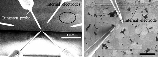
All of the samples used in the present study were prepared by the solid-state reaction method. Our samples were produced from reagent grade powders of ZnO and additives. ZnO-based varistors in this paper were produced using ZnO containing Bi2O3, Sb2O3, and small amounts of other elements, such as Co2O3, MnO2, NiO, Cr2O3, SiO2, Al2O3, and B2O3. The composition is a typical commercial formulation for practical varistors. Fabricated MLCVs were produced using the conventional multilayer ceramic process. Details on the synthesis condition of MLCVs are given in our previous papers.[ Reference Koga and Sawada 3 ] The green chips were constructed into 8.5 mm in length, 7.5 mm in width, and 4.0 mm in height. They have a structure in which, 30 varistor-layers and Ag-internal electrodes are alternately stacked. The sintered thickness of varistor-layers is about 50 µm between the internal electrodes. They were sintered at about 930 °C below the melting point of Ag (960 °C) in air. The resulting sintered chips were then terminated with Ag-based electrodes at 800 °C in air, and we finally obtained MLCVs of a size of 5.5, 5.0, and 3.0 mm in length, width, and height. Their V–I properties are evaluated using DC current from 1 µA to 1 mA, and voltages at the measured currents were defined as V 1 µA, V 10 µA, V 100 µA, and V 1 mA, respectively. Here, V 1 mA is usually termed varistor voltage, meaning breakdown voltage as a device. The non-linearity exponents α 10 µA were determined from V–I data, between current of 10 µA and 1 mA, according to the following equation: α 10 µA = (log I 1 mA − log I 10 µA)/(logV 1 mA − logV 10 µA). MLCVs studied have V 1 mA = 27 V, α 10 µA = 20 and capacitance = 30 nF at 1 kHz. Varistor voltage per a grain boundary (V gb) in MLCVs was determined from V 1 mA and an average grain size, which is measured by the intercept method from the microstructural observation [scanning electron microscope (SEM) images] of the cross-sectional surface in the same way as given in our previous paper.[ Reference Higashi, Hogiri and Koga 5 ] In addition, for electrically microstructural analysis, MLCVs were ground to approximately the mid plane with SiC papers and polished carefully with finer alumina powders. After polishing and drying, dry etching of CaF2 was performed for the polished surface of them. Under a SEM, one tungsten probe was directly contacted with each surface of two adjacent ZnO grains. It is confirmed experimentally that the contact between the ZnO grain and tungsten probe has no resistance (≈ 0 Ω), from the measurement using two probes in the surface of a ZnO grain. Electrical measurements of V–I behavior were then conducted for single-grain junctions between two adjacent ZnO grains using a nano-prober system, as shown in Fig. 1. The V–I measurement were performed at least two times to confirm superior data reproducibility. The dada were then analyzed in the present study.

Figure 1. SEM images of direct measurement of a single junction between ZnO grains using a nano-prober system.
Results and discussion
V–I characteristics for single junctions at grain boundaries around a ZnO grain
V–I behavior for three adjacent single junctions were measured across grain boundaries around a ZnO grain within the MLCV shown in Fig. 2. The results implied that direct measurement using a nano-prober is very available for the microstructural analysis of electrical properties in fine-grained varistors. Shown in Fig. 3 is V–I characteristics for the individual single junctions at each of three grain boundaries around a ZnO grain. Different behavior of V–I curve are clearly found to be obtained by changing only one side of the ZnO grain. The results on adjacent ZnO grains reveal that the three grain to grain junctions within the local microstructure (i.e., around a ZnO grain) possess not same but different V–I characteristics with the wide non-linearity variation of good to bad junctions. The junction area between grains not being known due to having a large variation of grain size in the microstructure, we are not able to similarly analyze them for an equal current density. Therefore, non-linearity of a single junction in the present study also was evaluated on the basis of the method by the former study.[ Reference Tao, Ai, Dorlanne and Loubiere 7 ] The maximum non-linear exponent (α max) is determined from α-values [α = (logI 2 − logI 1)/(logV 2 − logV 1)] in V–I property. A voltage corresponding to resulting α max is defined as V αmax, namely, a breakdown voltage at a grain boundary. V αmax and α max as non-linear index were thus characterized for each single junction. It is quantitatively shown from the result that the three junctions between the adjacent grains have considerable variations in V αmax of 2.1–2.7 and α max of 5.4–34.0 as summarized in Table I. The large variation of V–I behavior for the three junctions is found in fine-grained MLCVs as well as that of varistors consisting of large grains (150 µm) in the previous report.[ Reference Tao, Ai, Dorlanne and Loubiere 7 ] It is possible to say that the effect of ZnO grains on V–I property is very significant despite adjacent grains within narrow region. The electrical characteristics for a grain boundary has been analyzed for the simplified model of the boundary between bi-crystals joined by two ZnO single crystals.[ Reference Nakamura, Harada, Kuribara, Kishimoto, Motohira and Yanagida 8 , Reference Sato, Yamamoto and Ikuhara 9 ] The results reported in previous studies have demonstrated that the property of a single junction is able to be significantly influenced by the atomic structural relationship between two grains and by the electrical states (i.e., donor density) of each grain.[ Reference Tao, Ai, Dorlanne and Loubiere 7 – Reference Sato, Yamamoto and Ikuhara 9 ] Thus, the different V–I characteristics of the junctions around a ZnO grain probably is closely related to crystal orientation and/or donor concentrations of ZnO grains across a grain boundary. In addition, the grains in Bi-doped ZnO varistors consist of not only single crystal, but also twining, containing a very small amount of Co and donor (i.e., Al3+).[ Reference Chiang and Kingery 10 , Reference Inada 11 ] The presence of twined grains substructure has been reported to cause high non-linearity, because of other Schottky-type energy barriers comprising at twin grain boundaries.[ Reference Haskell, Souri and Helfand 12 , Reference Duran, Tartaj and Moure 13 ] Hence, the non-uniform behavior of three individual grain boundaries as shown in Fig. 3 may be attributed as well to the microstructure combined with two grain types of single and twinning crystal. However, the origin of non-linearity variation in single junctions of adjacent grains has yet to be fully elucidated in the present study. This will need to be further investigated by means of precise crystal-structural and electrical analysis of the microstructure.
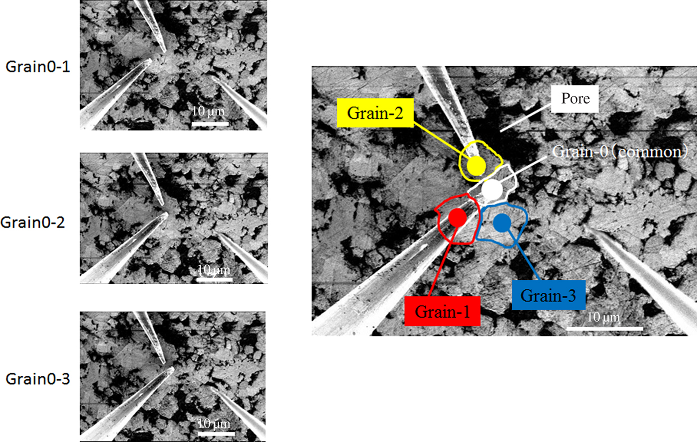
Figure 2. SEM images when measuring for three adjacent single junctions across grain boundaries around a ZnO grain within the MLCV.
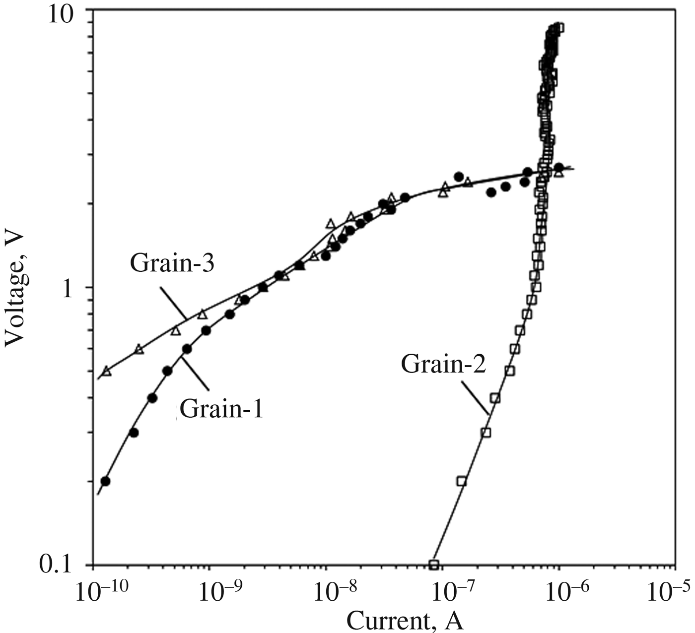
Figure 3. V–I curves of three single junctions between the common grain-0 and around the grain (−1, 2, and 3).
Table I. V αmax measured using nano-prober system and apparent V gb determined by V 1 mA and grain boundary numbers.

Variation in non-linearity of single junctions in MLCVs
V–I curves of single junctions (N = 30) selected randomly in the microstructure were examined for the fine-grained MLCV. The arithmetic means of V αmax and α max by the direct measurement are presented in Table I, with V gb (=V 1 mA/numbers of grain boundaries) given from V 1 mA as a device and the numbers of microstructural grain boundaries. In some cases, current through a back side of the measured grain surface may be detected in the present evaluation, thus we have compared with breakdown voltages at a grain boundary given by the different measurement method. It is evident from Table I that V αmax (=1.78 V) and V gb (=1.98 V) agree with each other because the difference between them is <10%. It has been confirmed from the result that they are in good agreement with each other regardless of the different measurement methods. Thus, we can say that direct measurement using a nano-prober system is a very useful means for electrical analysis of individual single junctions within fine-grained varistors. Further detailed examination of non-linear characteristics was then performed to characterize V αmax and α max by the direct measurement. The frequency distributions of V αmax and α max are presented in Fig. 4 [(A) V αmax and (B) α max], respectively. It should be noted that the results apparently demonstrate that both of the distributions are not only wide, but also asymmetrical in histograms. The wide asymmetry is suggested to result from the presence of several non-linear components in the microstructure. Similar distributions to V αmax and α max in fine-grained MLCVs are observed also in the results of ZnO varistors with large grains (150 µm), which were provided by the different measurement means using wire contacts from the present. The previous report has indicated that ZnO varistors with large grains have the wide non-linearity variation of good to bad junctions in the polycrystalline. Similarly, non-linear property of fine-grained MLCVs was found comprised their junctions with large variations in V αmax (=0.3–2.8 V) and α max (=1.1–44.0) as illustrated in histograms. Totaling of V–I characteristics for individual junctions given by a nano-prober system should be able to present the non-linear characteristics of MLCVs as a device. Hence, it is likely that a mean value of V αmax (=1.78 V) by the direct measurement would be good agreement with V gb (=1.98 V), which was estimated from the property of MLCVs and microstructural observation.
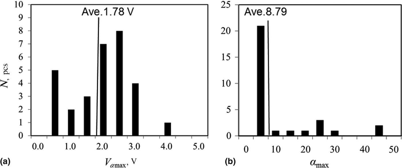
Figure 4. Frequency distributions of V αmax and α max [(a) V αmax and (b) α max].
To further examine their specific property in frequency distributions, a scatter diagram was plotted for V αmax versus α max. The result is shown in Fig. 5. It appears that the resulting relationship is able to be distinguished between at least two groups as good and bad junctions. Good junctions with high non-linearity of α max (e.g., ≥10) are found to have relatively high V αmax levels of about 1.8–2.8 V. On the other hand, bad junctions showing low α max (e.g., <10) seem to be composed of a lower V αmax range of 0.3–2.5 V. From their results, it is apparent that individual junctions in MLCVs are not uniform characteristics, irrespective of whether the microstructure of varistors is fine grained with an average size of 2 µm or not. The microstructure of MLCVs studied seems to have at least two types of good and bad junctions as mentioned above, and we are able to quote about 2.0 and 1.4 V as their mean values in the distributions, respectively. The difference of V αmax between them is clearly significant. From the numbers of two types, the numerical ratio of good to bad junctions is estimated to be about one to two within the present MLCVs, which is seen to be in rough agreement with that of the result shown in the previous study on varistors with large grains.[ Reference Tao, Ai, Dorlanne and Loubiere 7 ] The results imply that the ratio of good to bad junctions probably is independent of microstructural development as grain growth. The two types of junction characteristics are believed to be due to different barrier levels comprising the presence of two grain types (single and twinning) rather than effects of crystal orientation and donor concentrations of ZnO grains, as described above. However, the effect of grain structures on non-linearity of single junctions is not yet fully clarified; detailed investigation is further required.
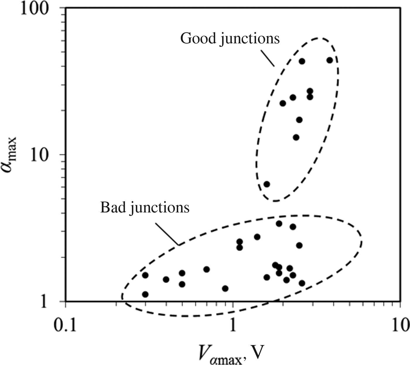
Figure 5. Scatter diagram for V αmax versus α max of single junctions.
In general, both non-linearity and stability against ESD are degraded with decreasing varistor voltage by reducing the number of grain boundaries.[ Reference Koga, Sawada, Amisawa, Minami and Okimoto 2 , Reference Koga and Sawada 3 ] The characteristic degradations with decreasing grain-boundary density should occur due to forming a low resistance path for electrical current to flow between internal electrodes. The similar path, which is continuously connected by bad junctions with large leakage current, would be able to affect not only non-linearity, but also the stability of MLCVs. Needless to say, the presence of bud junctions in the polycrystalline provides the decrement of non-linearity as MLCVs. Moreover, microstructural current densities should undoubtedly become extremely high concentration in the path region (i.e., bad junctions), thereby causing degradation of stability.
From results obtained, we thus believe that in electrical a sense, high-level uniformity of single junctions is intrinsically essential for improvement of protection performance and reliability rather than the fine-grained microstructure. Accordingly, decreasing non-linearity variation as bad junctions should play the crucial role in further characteristic improvement of MLCVs. The grain control of twinning as well as crystal orientation and donor concentration is considered effective in enhancing the non-linearity uniformity. There would be probability of further influence on the electrically microstructural control, by texture engineering using templated grain growth or magnetic field, sintering process such as millimeter heating, and synthesis from mechanically treated nano-composite particles.[ Reference Wada, Kakimoto and Ohsato 14 – Reference Tasaki, Tatami, Nakano, Wakihara, Komeya and Meguro 17 ]
Conclusions
In the present work, direct measurement of the electrical property of individual grain boundaries was performed for fine-grained MLCVs using a nano-prober system. Our findings from the experimental analysis are listed below. (i) Direct measurement using a nano-prober system is very available for the microstructural analysis of the electrical property in fine-gained varistors. (ii) The effect of ZnO grains on V–I property is very significant. The non-linearity variation probably is independent of microstructural development as grain growth. (iii) The microstructure of fine-grained MLCVs was found to be comprised of at least two non-linear types of good and bad junctions. The two junction characteristics are believed to be due to different barrier levels comprising the presence of two grain types (single and twinning) rather than effects of crystal orientation and donor concentrations of ZnO grains. Good junctions with high non-linearity of α max (e.g., ≥10) possess relatively high V αmax of 1.8–2.8 V. On the other hand, bad junctions showing low α max (e.g., <10) seem to be composed of a lower V αmax range of 0.3–2.5 V. The numerical ratio of good to bad junctions was estimated to be about one to two within the MLCVs studied.
In conclusion, it was found that individual single junctions in MLCVs are not uniform characteristics, regardless of fine grained, owing to non-linearity variation at grain boundaries in the polycrystalline. The experimental analysis implies that decreasing bad junctions of small non-linear coefficient is essential to enhance performance of MLCVs. The grain control of twinning as well as crystal orientation and donor concentration probably is effective in significantly improving performance of MLCVs and the electrical stability against ESD/LDS. However, until now, no work on varistors would have focused on the grain control for enhancement of the practical performance as a protection device. We therefore believe that to study the grain control technology within varistors should be an important theme for further improvement of MLCVs in the future.


