Hostname: page-component-8448b6f56d-42gr6 Total loading time: 0 Render date: 2024-04-18T10:42:41.331Z Has data issue: false hasContentIssue false

Efficiency enhancement via metal-coated porous amorphous silicon back reflectors incorporated in amorphous silicon solar cells

Published online by Cambridge University Press:  20 April 2016

Shweta Bhandaru
Affiliation:
Interdisciplinary Graduate Program in Material Science, Vanderbilt University, Nashville, TN 37235, USA
Angelo Bozzola
Affiliation:
Department of Physics, University of Pavia, via Bassi 6, I-27100 Pavia, Italy
Marco Liscidini*
Affiliation:
Department of Physics, University of Pavia, via Bassi 6, I-27100 Pavia, Italy
Sharon M. Weiss*
Affiliation:
Department of Electrical Engineering and Computer Science, Vanderbilt University, Nashville, TN 37235, USA
*
Address all correspondence to S.M. Weiss at sharon.weiss@vanderbilt.edu and M. Liscidini at marco.liscidini@unipv.it
Get access

Abstract

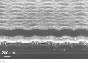
We present two straightforward and cost-effective methods, based on metal-assisted chemical etching and a direct imprinting technique, to fabricate metal-covered porous amorphous silicon back reflectors for amorphous silicon solar cells. We demonstrate an increase of approximately 30% in both short-circuit current and overall efficiency with respect to a cell with a flat metal back reflector. This is achieved by implementing light trapping via either a roughened porous amorphous silicon layer or an imprinted periodic grating. This work provides a pathway to increase amorphous silicon solar cell efficiency via increased absorption without significantly impacting processing costs.

Type
Plasmonics, Photonics, and Metamaterials Research Letter
Copyright
Copyright © Materials Research Society 2016 

Access options

Get access to the full version of this content by using one of the access options below. (Log in options will check for institutional or personal access. Content may require purchase if you do not have access.)

References

1. Xing, Y., Han, P., Wang, S., Liang, P., Lou, S., Zhang, Y., Hu, S., Zhu, H., Zhao, C., and Mi, Y.: A review of concentrator silicon solar cells. Renew. Sustain. Energy Rev. 51, 1697 (2015).CrossRefGoogle Scholar
2. Mousazadeh, H., Keyhani, A., Javadi, A., Mobli, H., Abrinia, K., and Sharifi, A.: A review of principle and sun-tracking methods for maximizing solar systems output. Renew. Sustain. Energy Rev. 13, 1800 (2009).CrossRefGoogle Scholar
3. Raut, H.K., Ganesh, V.A., Nair, A.S., and Ramakrishna, S.: Anti-reflective coatings: a critical, in-depth review. Energy Environ. Sci. 4, 3779 (2011).Google Scholar
4. Bozzola, A., Liscidini, M., and Andreani, L.C.: Photonic light-trapping versus Lambertian limits in thin film silicon solar cells with 1D and 2D periodic patterns. Opt. Express 20, A224 (2012).Google Scholar
5. Martins, E.R., Li, J., Liu, Y., Depauw, V., Chen, Z., Zhou, J., and Krauss, T.F.: Deterministic quasi-random nanostructures for photon control. Nat. Commun. 4, 2665 (2013).Google Scholar
6. Pratesi, F., Burresi, M., Riboli, F., Vynck, K., and Wiersma, D.S.: Disordered photonic structures for light harvesting in solar cells. Opt. Express 21, A460 (2013).Google Scholar
7. Trevino, J., Forestiere, C., Di Martino, G., Yerci, S., Priolo, F., and Dal Negro, L.: Plasmonic-photonic arrays with aperiodic spiral order for ultra-thin film solar cells. Opt. Express 20, A418 (2012).CrossRefGoogle ScholarPubMed
8. Jani, O., Ferguson, I., Honsberg, C., and Kurtz, S.: Design and characterization of GaN/InGaN solar cells. Appl. Phys. Lett. 91, 132117 (2007).Google Scholar
9. Gloeckler, M. and Sites, J.R.: Band-gap grading in Cu(In,Ga)Se2 solar cells. J. Phys. Chem. Solids 66, 1891 (2005).Google Scholar
10. Stadler, A.: Transparent conducting oxides—An up-to-date overview. Materials 5, 661 (2012).Google Scholar
11. Granqvist, C.G.: Transparent conductors as solar energy materials: a panoramic review. Sol. Energy Mater. Sol. Cells 91, 1529 (2007).Google Scholar
12. Green, M.A., Emery, K., Hishikawa, Y., Warta, W., and Dunlop, E.D.: Solar cell efficiency tables (version 47). Prog. Photovolt. Res. Appl. 24, 3 (2016).CrossRefGoogle Scholar
13.Solar accounts for 1% of global electricity, how long will the next 1% take?: http://www.pv-tech.org/editors-blog/solar_accounts_for_1_of_global_electricity_how_long_will_the_next_1_take (accessed December 30, 2015).Google Scholar
14. Müller, J., Rech, B., Springer, J., and Vanecek, M.: TCO and light trapping in silicon thin film solar cells. Sol. Energy 77, 917 (2004).Google Scholar
15. Curtin, B., Biswas, R., and Dalal, V.: Photonic crystal back reflectors for light management and enhanced absorption in amorphous silicon solar cells. Appl. Phys. Lett. 95, 231102 (2009).Google Scholar
16. Atwater, H.A. and Polman, A.: Plasmonics for improved photovoltaic devices. Nat. Mater. 9, 205 (2010).Google Scholar
17. Ryckman, J.D., Liscidini, M., Sipe, J.E., and Weiss, S.M.: Direct imprinting of porous substrates: a rapid and low-cost approach for patterning porous nanomaterials. Nano Lett. 11, 1857 (2011).Google Scholar
18. Liscidini, M., Gerace, D., Andreani, L.C., and Sipe, J.E.: Scattering-matrix analysis of periodically patterned multilayers with asymmetric unit cells and birefringent media. Phys. Rev. B 77, 035324 (2008).CrossRefGoogle Scholar
19. Andreani, L.C., Bozzola, A., Kowalczewski, P., and Liscidini, M.: Photonic light trapping and electrical transport in thin-film silicon solar cells. Sol. Energy Mat. Sol. C 135, 78 (2015).Google Scholar
20. Zanotto, S., Liscidini, M., and Andreani, L.C.: Light trapping regimes in thin-film silicon solar cells with a photonic pattern. Opt. Express 18, 4260 (2010).Google Scholar
21. Huang, Z., Geyer, N., Werner, P., de Boor, J., and Gösele, U.: Metal-assisted chemical etching of silicon: a review. Adv. Mater. 23, 285 (2011).CrossRefGoogle ScholarPubMed
22. Chartier, C., Bastide, S., and Lévy-Clément, C.: Metal-assisted chemical etching of silicon in HF–H2O2 . Electrochim. Acta 53, 5509 (2008).Google Scholar
23. Li, X.: Metal assisted chemical etching for high aspect ratio nanostructures: a review of characteristics and applications in photovoltaics. Curr. Opin. Solid State Mater. Sci. 16, 71 (2012).Google Scholar
24. Omampuliyur, R.S., Bhuiyan, M., Han, Z., Jing, Z., Li, L., Fitzgerald, E.A., Thompson, C.V., and Choi, W.K.: Nanostructured thin film silicon anodes for Li-ion microbatteries. J. Nanosci. Nanotechnol. 15, 4926 (2015).Google Scholar
25. Ishikawa, R., Kato, S., Yamazaki, T., Kurokawa, Y., Miyajima, S., and Kongai, M.: Solid-phase crystallization of amorphous silicon nanowire array and optical properties. Japan. J. Appl. Phys. 53, 02BE09 (2014).Google Scholar
26. Douani, R., Piret, G., Hadjersi, T., Chazalviel, J.-N., and Solomon, I.: Formation of a-Si:H and a-Si1−x C x :H nanowires by Ag-assisted electroless etching in aqueous HF/AgNO3 solution. Thin Solid Films 519, 5383 (2011).Google Scholar
27. Mares, J.W., Fain, J.S., Beavers, K.R., Duvall, C.L., and Weiss, S.M.: Shape-engineered multifunctional porous silicon nanoparticles by direct imprinting. Nanotechnology 26, 271001 (2015).Google Scholar
28. Kowalczewski, P., Liscidini, M., and Andreani, L.C.: Light trapping in thin-film solar cells with randomly rough and hybrid textures. Opt. Express 21, A808 (2013).Google Scholar
29. Battaglia, C., Hsu, C.-M., Söederströem, K., Escarré, J., Haug, F.-J., Charrière, M., Boccard, M., Despeisse, M., Alexander, D.T.L., Cantoni, M., Cui, Y., and Ballif, C.: Light trapping in solar cells: can periodic beat random. ACS Nano 6, 2790 (2012).Google Scholar
30. Green, M.A.: Lambertian light trapping in textured solar cells and light-emitting diodes: analytical solutions. Prog. Photovolt. Res. Appl. 10, 235 (2002).Google Scholar
Supplementary material: File

Bhandaru supplementary material

Bhandaru supplementary material 1

Download Bhandaru supplementary material(File)
File 1.4 MB