Hostname: page-component-8448b6f56d-cfpbc Total loading time: 0 Render date: 2024-04-18T04:43:48.665Z Has data issue: false hasContentIssue false

Effect of deposition pressure on the microstructure and thermoelectric properties of epitaxial ScN(001) thin films sputtered onto MgO(001) substrates

Published online by Cambridge University Press:  16 February 2015

Polina V. Burmistrova*
Affiliation:
School of Electrical and Computer Engineering, Purdue University, West Lafayette, Indiana 47907, USA; and Birck Nanotechnology Center, Purdue University, West Lafayette, Indiana 47907, USA
Dmitri N. Zakharov
Affiliation:
Birck Nanotechnology Center, Purdue University, West Lafayette, Indiana 47907, USA; and Brookhaven National Laboratory, Upton, New York 11974, USA
Tela Favaloro
Affiliation:
School of Engineering, University of California Santa Cruz, Santa Cruz, California 95064, USA
Amr Mohammed
Affiliation:
School of Electrical and Computer Engineering, Purdue University, West Lafayette, Indiana 47907, USA; and Birck Nanotechnology Center, Purdue University, West Lafayette, Indiana 47907, USA
Eric A. Stach
Affiliation:
Brookhaven National Laboratory, Upton, New York 11974, USA
Ali Shakouri
Affiliation:
School of Electrical and Computer Engineering, Purdue University, West Lafayette, Indiana 47907, USA; Birck Nanotechnology Center, Purdue University, West Lafayette, Indiana 47907, USA; and School of Engineering, University of California Santa Cruz, Santa Cruz, California 95064, USA
Timothy D. Sands
Affiliation:
School of Electrical and Computer Engineering, Purdue University, West Lafayette, Indiana 47907, USA; School of Materials Engineering, Purdue University, West Lafayette, Indiana 47907, USA; and Birck Nanotechnology Center, Purdue University, West Lafayette, Indiana 47907, USA
*
a)Address all correspondence to this author. e-mail: polina.burmistrova@stonybrook.edu
Get access

Abstract

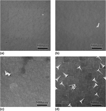
Four epitaxial ScN(001) thin films were successfully deposited on MgO(001) substrates by dc reactive magnetron sputtering at 2, 5, 10, and 20 mTorr in an Ar/N2 ambient atmosphere at 650 °C. The microstructure of the resultant films was analyzed by x-ray diffraction, scanning electron microscopy, and transmission electron microscopy. Electrical resistivity, electron mobility and concentration were measured using the room temperature Hall technique, and temperature dependent in-plain measurements of the thermoelectric properties of the ScN thin films were performed. The surface morphology and film crystallinity significantly degrade with increasing deposition pressure. The ScN thin film deposited at 20 mTorr exhibits the presence of <221> oriented secondary grains resulting in decreased electric properties and a low thermoelectric power factor of 0.5 W/mK2 at 800 K. The ScN thin films grown at 5 and 10 mTorr are single crystalline, yielding the power factor of approximately 2.5 W/mK2 at 800 K. The deposition performed at 2 mTorr produces the highest quality ScN thin film with the electron mobility of 98 cm2 V−1 s−1 and the power factor of 3.3 W/mK2 at 800 K.

Type
Articles
Copyright
Copyright © Materials Research Society 2015 

Access options

Get access to the full version of this content by using one of the access options below. (Log in options will check for institutional or personal access. Content may require purchase if you do not have access.)

References

REFERENCES

Gschneider, K.A., Melson, G.A., Melson, D.A., Youngblood, D.H., and Schock, H.H.: Scandium: Its Occurrence (Academic Press, London, 1975), p. 165.Google Scholar
Gall, D., Petrov, I., Madsen, L.D., Sundgren, J-E., and Greene, J.E.: Microstructure and electronic properties of the refractory semiconductor ScN grown on MgO(001) by ultra-high vacuum reactive magnetron sputter deposition. J. Vac. Sci. Technol., A 16, 2411 (1998).CrossRefGoogle Scholar
Gall, D., Stadele, M., Jarrendahl, K., Petrov, I., Desjardins, P., Haasch, R.T., Lee, T-Y., and Greene, J.E.: Electronic structure of ScN determined using optical spectroscopy, photoemission, and ab initio calculations. Phys. Rev. B 63, 125119 (2001).Google Scholar
Gall, D., Petrov, I., Hellgren, N., Hultman, L., Sundgren, J.E., and Greene, J.E.: Growth of poly- and single-crystal ScN on MgO(001): Role of low-energy N2+ irradiation in determining texture, microstructure evolution, and mechanical properties. J. Appl. Phys. 84, 6034 (1998).Google Scholar
Saha, B., Acharya, J., Sands, T.D., and Waghmare, U.V.: Electronic structure, phonons, and thermal properties of ScN, ZrN, and HfN: A first-principles study. J. Appl. Phys. 107, 033715 (2010).CrossRefGoogle Scholar
Moram, M.A., Barber, Z.H., and Humphreys, C.J.: The effect of oxygen incorporation in sputtered scandium nitride films. Thin Solid Films 516, 8569 (2008).Google Scholar
Dismukes, J.P., Yim, W.M., and Ban, V.S.: Epitaxial growth and properties of semiconducting ScN. J. Cryst. Growth 13, 365 (1972).CrossRefGoogle Scholar
Gregoire, J.M., Kirby, S.D., Scopelianos, G.E., Lee, F.H., and van Dover, R.B.: High mobility single crystalline ScN and single-orientation epitaxial YN on sapphire via magnetron sputtering. J. Appl. Phys. 104, 074913 (2008).Google Scholar
Gregoire, J.M., Kirby, S.D., Turk, M.E., and van Dover, R.B.: Structural, electronic and optical properties of (Sc, Y) N solid solutions. Thin Solid Films 517, 1607 (2009).CrossRefGoogle Scholar
Burmistrova, P.V., Maassen, J., Favaloro, T., Saha, B., Salamat, S., Koh, Y.R., Lundstrom, K.S., Shakouri, A., and Sands, T.D.: Thermoelectric properties of epitaxial ScN films deposited by reactive magnetron sputtering onto MgO(100) substrates. J. Appl. Phys. 113, 153704 (2013).CrossRefGoogle Scholar
Kerdsongpanya, S., van Nong, N., Pryds, N., Zukauskaite, A., Jensen, J., Birch, J., Lu, J., Hultman, L., Wingqvist, G., and Eklund, P.: Anomalously high thermoelectric power factor in epitaxial ScN thin films. Appl. Phys. Lett. 99, 232113 (2011).CrossRefGoogle Scholar
Moram, M.A., Novikov, S.V., Kent, A.J., Nörenberg, C., Foxon, C.T., and Humphreys, C.J.: Growth of epitaxial thin films of scandium nitride on 100-oriented silicon. J. Cryst. Growth 310, 2746 (2008).Google Scholar
King, S.W., Davis, R.F., and Nemanich, R.J.: Gas source molecular beam epitaxy of scandium nitride on silicon carbide and gallium nitride surfaces. J. Vac. Sci. Technol., A 32, 061504 (2014).Google Scholar
King, S.W., Nemanich, R.J., and Davis, R.J.: Valence and conduction band alignment at ScN interfaces with 3C-SiC (111) and 2H-GaN (0001). Appl. Phys. Lett. 105, 081606 (2014).Google Scholar
Oshima, Y., Villora, E.G., and Shimamura, K.: Hydride vapor phase epitaxy and characterization of high-quality ScN epilayers. J. Appl. Phys. 115, 153508 (2014).CrossRefGoogle Scholar
Kerdsongpanya, S., Alling, B., and Eklund, P.: Effect of point defects on the electronic density of states of ScN studied by first-principles calculations and implications for thermoelectric properties. Phys. Rev. B 86, 195140 (2012).CrossRefGoogle Scholar
Moram, M.A., Joyce, T.B., Chalker, P.R., Barber, Z.H., and Humphreys, C.J.: Microstructure of epitaxial scandium nitride films grown on silicon. Appl. Surf. Sci. 252, 8385 (2006).Google Scholar
Moram, M.A., Kappers, M.J., and Humphreys, C.J.: Low dislocation density nonpolar (11–20) GaN films achieved using scandium nitride interlayers. Phys. Status Solidi C 7, 1778 (2010).CrossRefGoogle Scholar
Moram, M.A., Zhang, Y., Kappers, M.J., Barber, Z.H., and Humphreys, C.J.: Dislocation reduction in gallium nitride films using scandium nitride interlayers. Appl. Phys. Lett. 91, 152101 (2007).Google Scholar
Zebarjadi, M., Bian, Z., Singh, R., Shakouri, A., Wortman, R., Rawat, V., and Sands, T.: Thermoelectric transport in a ZrN/ScN superlattice. J. Electron. Mater. 38, 960 (2009).CrossRefGoogle Scholar
Rawat, V. and Sands, T.D.: Growth of TiN/GaN metal/semiconductor multilayers by reactive pulsed laser deposition. J. Appl. Phys. 100, 064901 (2006).CrossRefGoogle Scholar
Rawat, V., Koh, Y.K., Cahill, D.G., and Sands, T.D.: Thermal conductivity of (Zr,W)N/ScN metal/semiconductor multilayers and superlattices. J. Appl. Phys. 105, 024909 (2009).CrossRefGoogle Scholar
Kerdsongpanya, S., Alling, B., and Eklund, P.: Phase stability of ScN-based solid solutions for thermoelectric applications from first-principles calculations. J. Appl. Phys. 114, 073512 (2013).CrossRefGoogle Scholar
Deng, R., Evans, S.R., and Gall, D.: Bandgap in Al1-xScxN. Appl. Phys. Lett. 102, 112103 (2013).Google Scholar
Hoglund, C., Bareno, J., Birch, J., Alling, B., Czigany, Z., and Hultman, L.: Cubic Sc1−x Al x N solid solution thin films deposited by reactive magnetron sputter epitaxy onto ScN(111). J. Appl. Phys. 105, 113517 (2009).Google Scholar
Hoglund, C., Birch, J., Alling, B., Bareno, J., Czigany, Z., Persson, P.O.A., Wingqvist, G., Zukauskaite, A., and Hultman, L.: Increased electromechanical coupling in w-ScxAl1-xN. J. Appl. Phys. 107, 1235515 (2010).Google Scholar
Moram, M.A. and Zhang, S.: ScGaN and ScAlN: Emerging nitride materials. J. Mater. Chem. A 17, 6042 (2014).Google Scholar
Burmistrova, P.V.: Microstructure and thermoelectric properties of ScN thin films and metal/ScN superlattices for high-temperature energy conversion. Ph.D. Dissertation, Purdue University, West Lafayette, 2014.Google Scholar
Gall, D., Petrov, I., Desjardins, P., and Greene, J.E.: Microstructural evolution and Poisson ratio of epitaxial ScN grown on TiN(001)/MgO(001) by ultra-high vacuum reactive magnetron sputter deposition. J. Appl. Phys. 86, 5524 (1999).Google Scholar
Stroscio, J.A., Pierce, D.T., Stiles, M.D., Zangwill, A., and Sander, L.M.: Coarsening of unstable surface features during Fe (001) homoepitaxy. Phys. Rev. Lett. 75, 4246 (1995).CrossRefGoogle ScholarPubMed
Karr, B.W., Petrov, I., Cahill, D.G., and Greene, J.E.: Morphology of epitaxial TiN(001) grown by magnetron sputtering. Appl. Phys. Lett. 70, 1703 (1997).Google Scholar
Lee, N.E., Cahill, D.G., and Greene, J.E.: Evolution of surface roughness in epitaxial Si0.7Ge0.3(001) as a function of growth temperature (200-600°C) and Si(001) substrate miscut. J. Appl. Phys. 80, 2199 (1996).Google Scholar
Ehrlich, G. and Hudda, F.G.: Atomic view of surface self-diffusion: Tungsten on tungsten. J. Chem. Phys. 44, 1039 (1966).CrossRefGoogle Scholar
Wang, S.C. and Ehrlich, G.: Adatom motion to lattice steps: A direct view. Phys. Rev. Lett. 70, 41 (1993).CrossRefGoogle ScholarPubMed
Golzhauser, A. and Ehrlich, G.: Atom movement and binding on surface clusters: Pt on Pt(111) clusters. Phys. Rev. Lett. 77, 1334 (1996).Google Scholar
Leal, F.F., Ferreira, S.C., and Ferreira, S.O.: Modelling of epitaxial film growth with an Ehrlich-Schwoebel barrier dependent on the step height. J. Phys.: Condens. Matter 23, 292201 (2011).Google Scholar
Burstein, E.: Anomalous optical absorption limit in InSb. Phys. Rev. 93, 632 (1954).Google Scholar