

The 2011 Materials Research Society Spring Meeting, held in San Francisco on April 25–29, hosted over 5000 attendees for a program of 50 technical symposia, along with a plenary address and award lectures, an exhibit of over 120 companies and a technology innovation forum, a special forum by Acta Materialia, a Women in Materials Science & Engineering Breakfast, special programs in advocacy and materials science education and outreach, government funding sessions, professional development seminars, and a career center. For four nights, the Meeting also presented the MRS Late Show: a four-part television series, MAKING STUFF—Stronger, Smaller, Cleaner, and Smarter, produced by NOVA in cooperation with MRS.
Meeting Chairs Ping Chen (Dalian Institute of Chemical Physics, China), Chang Beom-Eom (University of Wisconsin—Madison, USA), Samuel S. Mao (Lawrence Berkeley National Laboratory, USA), and Ryan O’Hayre (Colorado School of Mines, USA) broadly divided the technical program into the areas of materials for energy and sustainability, electronic and photonic materials, nanomaterials and nanotechnology, and organic and biomaterials as well as other general materials science areas.
Energy Focus
This year, some emphasis was given to the role of materials in energy and sustainability, beginning with the plenary address given by Yet-Ming Chiang of the Massachusetts Institute of Technology and co-founder of A123 Systems who spoke on battery-powered energy storage for transportation and grid scale applications (see section, “Special talks and events”). The cluster of symposia on energy and sustainability focused on photovoltaics, energy conversion and storage, solid-state ionics and complex oxides, thermoelectrics, and electrochromics.
Solar cells on the rise
International attention on alternative energy resources has resulted in a range of materials paradigms targeted at improving solar energy conversion. This motivation for symposium B on third-generation and emerging solar cell technologies captured the attention of those engaged in fundamental physics research as well as groups focusing on technological implementation. One topic that generated a great deal of interest was the role of quantum confinement in designing new ways to improve photovoltaic (PV) efficiency. The physics and technological efficacy of multiple-exciton generation (carrier multiplication) and quantum cutting were scrutinized and debated, with new results presented for PbS, PbSe quantum dots, and for silicon nanocrystals embedded in SiO2. The important role of surface treatments on multiple-exciton generation and on exciton transport was also taken up in a number of talks and posters. In addition, new paradigms with enhanced charge collection efficiencies were elucidated for organic systems, quantum dot sensitized bulk materials, and ultrathin nanowires. A take-away message of the symposium was that quantum confinement can be exploited in a number of novel ways to tip the scales on competing relaxation mechanisms. By doing so, the efficiency of next-generation solar cells can be significantly improved.
A major application of thin-film silicon is in photovoltaic solar energy. Although manufacturing cost is expected to be low for thin-film silicon solar panels, relatively low conversion efficiency compared to crystalline silicon and other compound crystalline thin film solar panels is the major challenge for thin film silicon solar technology. Symposium A on amorphous and polycrystalline thin-film silicon science and technology focused on efficiency. Both microcrystalline (μc-Si:H) silicon or nanocrystalline silicon (nc-Si:H) offer the potential for improving cell efficiencies. F. Finger (Forschungszentrum Jülich, Germany) reviewed recent efficiency improvements in μc-Si:H solar cells with an emphasis on μc-SiC:H- and μc-SiO:H-doped layers and effective light management. Finger expects that over 14% efficiency with a-Si:H/μc-Si:H tandem solar cells will be attained soon. M. Zeman (Delft University of Technology, the Netherlands) showed that 23% efficiency is achievable using a-SiC:H/a-SiGe:H/nc-Si:H triple-junction structure with advanced light trapping to enhance photon harvesting. Along this line, many new light trapping and light management approaches have been investigated, including plasmonic light scattering using metal and dielectric nanoparticles and photonic structures. Theoretical and simulation studies show that the classical limit of 4n 2, where n is the refractive index, can be exceeded using advanced light trapping techniques. T. Matsui (AIST, Japan) presented their recent progress in developing μc-SiGe:H materials as low bandgap materials to absorb long wavelength light, which provides a new material for high efficiency solar cells. Significant progress in advancing the nc-Si:H technology for mass production has been made. A. Banerjee of United Solar Ovonic LLC (Michigan, USA) reported achieving initial 12% and stable 11.2% encapsulated module (400 cm2) efficiencies with an a-Si:H/nc-Si:H/nc-Si:H triple-junction structure, which are new world records for thin-film silicon solar modules as measured by the U.S. National Renewable Energy Laboratory.
A group of researchers from Carnegie Mellon University, University of California–Santa Cruz, and NASA have developed a laboratory version of a fiber lighting/PV device using composite materials. This lighting/PV multifunctional device has the advantage of high efficiency light usage. These cells can be created without using expensive electronic-grade silicon, resulting in both an efficient and economical solar cell. To maximize efficiency, the absorption layer absorbs both the visible and infrared (IR) regions of the electromagnetic spectrum. As reported in symposium E on energy harvesting, PbS quantum dots (with strong IR absorbance) are placed onto TiO2 nanotubes (having strong UV absorbance) using chemical deposition techniques to achieve a broad absorption spectrum. The conducting polymer poly(3-hexylthiophene) (P3HT) is also added to improve visible absorption and promote electron injection into the nanotubes. PbS and P3HT were also chosen for their bandgap energies that favorably align with the TiO2 nanotubes, further increasing the transfer of excited electrons into the nanotubes.
The future looks bright for organic photovoltaics, according to Yang Yang whose laboratory at the University of California–Los Angeles has made major contributions toward developing processing techniques that have steadily increased the overall power conversion efficiency of these next- generation solar cell technologies. Peak power conversion efficiencies in the 5–6 % range are commonly reported by academic researchers working on these systems, but it is rumored, said Yang, that the Mitsubishi Chemical company has developed a 9% efficiency device. “This brings us closer to the cost-competitive 10% efficiency mark,” said Yang in symposium CC on hybrid interfaces and devices. “But,” he said, “I would say 12% is a better number. If I can make a 12% efficient organic solar cell…then I can retire.” Yang reported that in addition to the TiO2 interfacial layer, his group uses a modified poly(3,4-ethylenedioxythiophene) layer (m-PEDOT) which is thicker, transparent, and has conductivities up to 100 S/cm2. Yang’s modified PEDOT layer also protects the device from solvent penetration, yet another challenge involved in processing multiple layers of these organic solar cells.
2011 Materials Research Society Spring Meeting Symposium Support
Acree Technologies, Inc.
Agilent Technologies UK, Ltd.
Air Force Office of Scientific Research
Air Force Research Laboratory
Air Liquide
Air Products
AIXTRON SE
Annealsys
Applied Materials, Inc.
Asociacion de la Industria Novarra
Asylum Research
Australian Nuclear Science and Technology Organisation (ANSTO)
AXPO Holding AG
Cengage Learning Global Engineering
CrysTec GmbH
Defense Threat Reduction Agency (DTRA)
Dow Chemical Company
E.A. Fischione Instruments, Inc.
E.I. DuPont de Nemours and Co., Inc.
Elsevier, Ltd.
EMPA Laboratory for High Performance Ceramics
FEI Company
General Electric—Global Research
GLOBALFOUNDRIES
HORIBA Jobin Yvon, Inc.
IBM Almaden Research Center
IBM Research Zurich
International Center for Materials NanoArchitectonics, National Institute for Materials Science
Impact Coatings AB
Institute for Materials Research (IMO)/IMOMEC-Hasselt University/IMEC vzw
IQE, Inc.
ITRI
JEOL USA, Inc.
JSR Micro, Inc.
Lawrence Berkeley National Laboratory, Department of Energy Office of Science
Lawrence Livermore National Laboratory
Kurt J. Lesker Company
M. Watanabe & Co., Ltd.
Medtronic, Inc.
Metal Estalki, S.L.
Montana State University, Chemical & Biological Engineering
Nanosystems Initiative Munich (NIM)
NANOVEA
NASA
National Electrostatics Corporation
National Institute of Standards and Technology
National Renewable Energy Laboratory
National Science Foundation
National Science Foundation, Thermal Transport Processes Program
Naval Research Laboratory, Solid State Devices Branch
NT-MDT Co.
Oak Ridge National Laboratory
Office of Naval Research
Omicron NanoTechnology USA
PANalytical, Inc.
Park Systems, Inc.
Princeton Center for Complex Materials
Purdue University, School of Materials Engineering, School of Biomedical Engineering
Quantachrome Instruments
Radiant Technologies, Inc.
Renewable Energy Materials Research Science and Engineering Center-Colorado School of Mines/NREL
RHK Technology, Inc.
RMIT University, Australia
Rocky Mountain Vacuum Tech, Inc.
Sandia National Laboratories
Sandvik AB
Seki Technotron USA
Semprus BioSciences
Sigma-Aldrich
Society for Biomaterials
Solexant, Inc.
SPECS Surface Nano Analysis GmbH
Strategic Analysis, Inc.
SuperPower, Inc.
Technische Universität München
Tokyo Electron America, Inc.
Transmill Technologies, Inc.
ULVAC Technologies, Inc.
United Solar Ovonic LLC
Universal Systems Co., Ltd.
UOP LLC
U.S. Department of Energy
Veeco
In the same symposium, Michael McGehee (Stanford University) discussed the role of “pore-filling” on the performance of solid-state dye-sensitized solar cells (DSSC), a technology originally developed by Michael Grätzel’s group (École Polytechnique Fédérale de Lausanne). The solid state version of DSSCs do not need liquid electrolytes, which makes them more compatible with conventional printing and coating techniques. However, for making efficient devices, it is necessary to ensure that the hole transporter (Spiro-OMeTAD) used to replace the electrolyte fills at least “half the volume” of the pores in the nanoporous TiO2 electron transport layer. With increased pore filling, the Spiro-OMeTAD also makes better contact with the dye molecules, thereby optimizing device performance. The main message from McGehee’s talk was that although pore-filling is important, “100 % pore filling is not necessary and in fact will not significantly improve solar cell efficiency, as previously believed.” His talk combined results from photovoltaic device characterization tests with x-ray photoelectron spectroscopy and transient photo-voltage measurements to substantiate this statement. McGehee’s group also demonstrated a novel plasmonic version of these devices in which metal nanoparticles significantly enhance electromagnetic field strengths, resulting in improved solar spectrum absorption. Their innovative approach uses a “dome shaped stamp” to easily pattern the TiO2 surface without need for complicated (and expensive) lithography techniques.
Band alignment is critical for charge transfer in organic solar cell devices, particularly hybrid organic–inorganic devices. However, without accurate techniques to measure these band energy values, it becomes extremely difficult to study and improve current understanding of these systems. So symposium CC’s invited speaker Julia Hsu (University of Texas) described how she used Kelvin probe measurements and photo-electron spectroscopy in air (PESA) to measure the Fermi levels and work functions (metals) and ionization potentials (semiconductors). Her group perfected these techniques to study materials like organic hole conducting polymers (P3HT), organic molecules like [6,6]-phenyl-C61-butyric acid methyl ester (PCBM), and inorganic materials like ZnO. Her goal is to eventually formulate a more plausible explanation for why P3HT-ZnO-based organic–inorganic hybrid solar cell systems have poor solar energy conversion efficiencies compared to their all-organic P3HT-PCBM counterparts. The research Hsu described was based on work done while she was at Sandia National Laboratories.
Hydrogen storage
Hydrogen storage and carbon dioxide capture are two glaring technical hurdles that impose an impasse on the implementation of several clean technologies, such as hydrogen fuel cells and advanced power generation processes, that could dramatically increase the use of cleaner energy and reduce greenhouse gas emissions. One of the most investigated materials for reversible hydrogen storage for different applications are the borohydrides with high hydrogen content up to 19%, but slow kinetics at high operation temperatures. To address this fundamental issue in symposium N on hydrogen storage and carbon-capture technologies, M. Chong of C. Jensen’s group at the University of Hawaii revealed that Mg(BH4)2 can be reversibly dehydrogenated to Mg(B3H8)2 in the range of 200-250°C thus providing the first example of a boron-based hydrogen storage material that undergoes direct hydrogen cycling at temperatures below 350 °C.
Aluminum hydride, AlH3, is one of the most promising H-storage materials with 10 wt% H2 content released at fuel cell operating temperatures. A cost- and heat-effective route to electrochemically synthesize AlH3 was demonstrated—as discussed by R. Zidan of Savannah River National Laboratory, USA—thus closing the reversible cycle for regeneration, a long sought-after path to realize this material for practical applications.
Other avenues to energy
A number of presentations were given on the application of nanomaterials to batteries and other applications where lower cost and weight are desired. L. Hu of Stanford University spoke about how replacing the metallic (copper and aluminum) mesh current collectors used in conventional lithium ion batteries can reduce their weight by 20–30%. But there is another advantage, Hu said in symposium F on renewable fuels and nanotechnology. Paper is made up of cellulose nanofibers that have a hierarchical structure. These nanoscale pathways can also be used to manipulate the transport of ions and electrons, resulting in more efficient batteries for energy storage. In order to accomplish this, however, paper has to be made electrically conductive using a stable carbon nanotube or graphene-based ink. The same approach can be transferred to textile fabrics to realize wearable textile-based electronics. Hu and his colleagues also demonstrated a MnO2-based textile pseudocapacitor that can be made at a substantially lower cost than other supercapacitors.
Drawing on almost four decades of materials research experience in nanomaterials, Mildred Dresselhaus (Massachusetts Institute of Technology) stated that nanostructured materials are increasingly important because they have many properties that are missing from other materials. In symposium I on nanoscale heat transfer, Dresselhaus said that high surface area, a crucial attribute of catalysts, is one such property. “The development of efficient, inexpensive catalysts is crucial for energy,” she said, “because so much of energy depends on catalytic conversion.” For nanothermoelectricity, the goal is to increase the electrical conductivity and decrease the thermal conductivity of materials. The greatest success so far has come from decreasing thermal conductivity. She gave an overview of four approaches that are being pursued toward this end by different researchers in the field: (1) targeting and eliminating specific phonons in a material that are contributing to high thermal conductivity; (2) using ballistic transport to move the phonons through the material without carrying much heat; (3) modulating the doping of grains in a nanothermoelectric material instead of overdoping, thereby producing a high carrier density without a lot of scattering; and (4) using density functional theory modeling to select sites in the material at which to preferentially insert dopants. This could help researchers determine what dopants to use, where to put them, and when to stop doping to avoid the diminishing returns of overdoping.
Organic and functional polymeric materials may offer an economic alternative to inorganic materials for applications in technologies that would enable the use of a renewable energy source and the use of present energy sources more efficiently. In symposium OO on organic and polymeric materials for semiconductor applications, F. So of the University of Florida discussed his research on down-conversion organic light-emitting diodes. Down conversion was first demonstrated by General Electric about a decade ago, and Osram had success with a similar approach using Firpic, a commercially available blue emitter. So modified that method in order to achieve a down-conversion organic light-emitting diode with better white emission. The challenge, he said, is that the emission spectrum of Firpic is not a close match for the excitation spectrum of the phosphor used for down conversion. He reported success in using microcavity structures to tune the excitation spectra of the phosphor, with a maximum efficiency of 68 lm/W for a red-yellow phosphor mixture. With the addition of a lens to improve light extraction, an efficiency of 99 lm/W was achieved.
The 2011 Spring Meeting Chairs awarded prizes for the following best poster presentations: (Q6.15) Nonvolatile and programmable nanowire circuits for nanoprocessors, H.S. Choe, H. Yan, S.W. Nam, Y. Hu, and C.M. Lieber of Harvard University, USA and S. Das, J.F. Klemic, and J.C. Ellenbogen of the MITRE Corporation, USA; (Q9.1) Oxygen migration at Pt or Cu/HfO2 interface under bias operation: Oxide based ReRAM application, T. Nagata, M. Haemori, Y. Yamashita, H. Yoshikawa, K. Kobayashi, Y. Iwashita, and T. Chikyow of the National Institute for Materials Science, Japan; (Y10.9) Field emission from atomically thin edges of reduced graphene oxide, H. Yamaguchi, J. Boisse, and M. Chhowalla of Rutgers University, USA; K. Murakami, F. Wakaya, and M. Takai of Osaka University, Japan; G. Eda of Imperial College London, UK; T. Fujita, P. Guan, and M. Chen of Tohoku University, Japan; and K. Cho and Y. Chabal of the University of Texas at Dallas, USA; (BB9.3) Contact thermal resistance between individual multi-walled carbon nanotubes, Y. Yang, S.W. Waltermire, and D. Li of Vanderbilt University, USA; J. Yang of Vanderbilt and Southeast University, China; Y. Chen of Southeast University; and T.T. Xu of the University of North Carolina at Charlotte, USA; (GG10.22) Low cost, environmentally benign patterning nanostructured TiO2 thin films, J.D. Bass, C.T. Rettner, N. Arellano, X. Ai, Q. Song, C. Scott, R.D. Miller, and H.-C. Kim of IBM Almaden Research Center, USA; C.D. Schaper of Transfer Devices, Inc., USA; and F.H. Alharbi of King Abdulaziz City for Science and Technology, Saudi Arabia; (PP3.14) Facile patterning of genetically engineered M13 bacteriophage for directional growth of human fibroblast cells, S.Y. Yoo, W.-J. Chung, and S.-W. Lee of the University of California–Berkeley and Lawrence Berkeley National Laboratory, USA and T.H. Kim of UC–Berkeley; (QQ9.63) Hysteresis-free operation of carbon nanotube based ferroelectric field-effect transistor, Y.S. Choi, J.-W. Sung, S.J. Kang, and C. Park of Yonsei University, Korea; (WW5.17) Piezoelecric force microscopy of crystalline oxide-semiconductor heterostructures, M.S. Marshall, J.W. Reiner, D. Kumah, F.J. Walker, and C.H. Ahn of Yale University, USA and P. Maksymovych and A.P. Baddorf of Oak Ridge National Laboratory, USA; (WW11.50) Ferroelectric polarization and domain structure in tetragonal phase BFO thin film, J. Zhang and R. Ramesh of the University of California–Berkeley, USA; and (XX6.10) Improving functional properties of amorphous silicone polymers with simulation, P.T. Shemella, T. Laino, and A. Curioni of IBM Research-Zurich, Switzerland and O. Fritz of ABB Corporate Research, Switzerland.
Nano Focus
Negative-index metamaterials (NIMs), synthetic materials with a negative index of refraction, have been demonstrated in two dimensions and in the microwave. Debashis Chanda of the University of Illinois at Urbana-Champaign gave a presentation about their work on the printing of NIMs. Three-dimensional NIMs have previously been created by layer-by-layer electron-beam lithography and focused ion-beam milling, but these techniques are too slow to scale to large-area production. Optical-range applications would require 3D NIMs with inch-scale dimensions and feature sizes on the order of hundreds of nanometers. Chanda reported the fabrication of such NIM structures with a simple stamping process. The group used a silicon stamp to produce an inch-square NIM structure with approximately 200 nm feature size. The robustness of the technique was demonstrated by scaling up to a 4-inch square, stamping both rigid and flexible substrates, confirming stamp reusability, creating a quasi-free-standing printed NIM, and tuning the feature size to approximately 180 nm. Optical measurements confirmed negative refraction in both three-layer and eleven-layer samples.
Nanopore-based devices are a versatile platform for single-molecule detection and analysis, and hold promise for ultrafast, inexpensive DNA sequencing. A DNA molecule, electrophoretically driven through a nanoscale pore, is highly confined and linearized within the nanopore constriction, allowing for the DNA molecule unfolding and subsequent interrogation. One roadblock to achieving the long promised nanopore single-molecule sequencing goal might be lifted with the advent of graphene nanopores. Graphene’s effective thickness in water was measured to be less than one nanometer and together with graphene’s excellent electrical conductivity, opens up the possibility to use graphene nanopores in single molecule DNA sequencing. In symposium AA on micro- and nanofluidic systems, S. Garaj (Harvard University) presented how technically challenging nanopores can be fabricated in the atomically thin graphene membranes. He stressed the importance of the imaging and accelerating voltage, quality of the graphene, and absence of contaminants in the fabrication of the high-quality graphene nanopores. Only graphene pores free from hydrocarbon contaminates are able to reach their full potential. In addition, Garaj demonstrated superior graphene nanopore resolution of the DNA size and DNA conformation detection compared to existing solid-state nanopores. He concluded that there are numerous avenues to explore using graphene within the framework of nanopore sensing, such as graphene as an electrode to control the local electric potential and translocation rates, or as an electrode to monitor the transverse conductance of individual nucleotides as they pass through a pore.
Graduate Students Receive Gold and Silver Awards
Graduate Student Awards were announced during the awards ceremony on April 27 at the 2011 Materials Research Society Spring Meeting in San Francisco.
Gold Graduate Student Awards (top) were awarded to (front row, left to right): Imogen Pryce (California Institute of Technology), Vivian Ferry (California Institute of Technology), and Charina Choi (University of California, Berkeley); and (back row, left to right): Jonathan Rivnay (Stanford University), Edward Barnard (Stanford University), Volker Sorger (University of California, Berkeley), Nathaniel Huebsch (Harvard University), SungWoo Nam (Harvard University), and June Hyuk Lee (Pennsylvania State University).
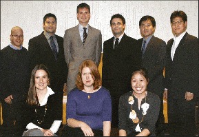
Silver Graduate Student Awards (right) were awarded to (first row, left to right): Laura Povlich (University of Michigan), Ingrid Koslow (University of California, Santa Barbara), Desalegne Teweldebrhan (University of California, Riverside); (second row, left to right): Vismadeb Mazumder (Brown University), Xi He (University of Nebraska, Lincoln), Thomas Kempa (Harvard University); (third row, left to right): Joel Grim (Wake Forest University), Sung Keun Lim (Massachusetts Institute of Technology), Qiao Zhang (University of California, Riverside), Takeaki Yajima (The University of Tokyo), and Jaemyung Kim (Northwestern University); (fourth row, left to right): Teng He (Dalian Institute of Chemical Physics, CAS), Francisco Lopez (Northwestern University), Wu Zhou (Lehigh University), Victor Acosta (University of California, Berkeley) and Yijin Kang (University of Pennsylvania); and (fifth row, left to right): Justin Koepsel (University of Wisconsin, Madison), Hyungsoon Im (University of Minnesota), and Dong Rip Kim (Stanford University).

Bio Focus
There has been increasing interest in using stem cell microenvironments, or niches, for controlling stem cell differentiation in tissue engineering applications. In particular, there is a need to develop tools to spatially and temporally regulate signals. As reported in symposium PP on engineering polymers for stem cell regulation and regenerative medicine, K. Anseth’s group (University of Colorado and Howard Hughes Medical Institute) has developed a number of orthogonal chemistries for directed modification of the local environment that surrounds cells. For example, cells were encapsulated in hydrogels and cell outgrowth was directed through two sequential events. First, the gels were degraded through the use of a photodegradable crosslinker. Next, thiolene chemistry was used to add in cell-adhesive peptides to promote outgrowth of cells to specific locations.
Cells are routinely cultured in two-dimensional environments, but recent studies demonstrate that cells behave differently in two-dimensional versus three-dimensional environments. As reported in symposium PP, C.G. Simon’s group (National Institute of Standards and Technology) has screened a number of 3D polymer scaffolds to evaluate their effect on mesenchymal stem cell differentiation to the osteogenic fate. In particular, different fabrication techniques were used to mold poly(ε-caprolactone) into scaffolds with varying topography. The nanofibrous scaffolds were found to promote osteogenesis in the absence of osteogenic supplements. Furthermore, the ability of nanofibers to support osteogenesis was confirmed using a different polymer composition.
Amphiphilic peptides have the capacity to self-assemble in ways that, if controlled, could lead to an array of potential applications. As reported in symposium JJ on hybrid inorganic–biological materials for life sciences applications, S. Stupp’s group (Northwestern University) injected such peptide amphiphile molecules, which can self-assemble to display the laminin epitope IKVAV that is a bioactive peptide amphiphile, into the spinal cord of a model animal with spinal nerve injury. The results showed an improvement in recovery that demonstrates that the peptide amphiphile molecules initiate the plasticity of serotonergic fibers post spinal cord injury. To understand the underlying mechanisms of this phenomenon, the number of serotonergic fibers in the injured spinal cord was compared in animals receiving bioactive versus a nonbioactive peptide amphiphile. The density of the serotonergic fibers was significantly higher for the group injected with the bioactive peptide amphiphile (IKVAV). The IKVAV peptide amphiphile-injected groups had a higher number of neurons at the injury site and a higher number of long propriospinal tract connections from the lumbar to the thoracic cord.
Tremendous activity has been registered in the past years in the area of biologically inspired synthesis of inorganic materials. This explosive growth was triggered by the needs related to cost reduction, high efficiency, and environmental safety in materials synthesis. Biomineralized materials are also known to be able to be synthesized with high control over a complex range of microstructures and morphologies. In symposium JJ, D. Morse (University of California–Santa Barbara) presented the biologically inspired fabrication of metal oxides at the nanoscale. In one example, Morse described the bio-inspired fabrication of the binary metal oxide BaTiO3. Traditionally, such perovskites are synthesized through classical ceramic technologies and at high temperatures, leading to difficulty in maintaining nanosized morphologies. The principles of biomineralization that can be harnessed for the fabrication of synthetic nanostructured complex oxides were presented.
Special talks and events
Plenary address on challenges for electrochemical storage
Yet-Ming Chiang of the Massachusetts Institute of Technology discussed the latest news from the world of battery-powered energy storage for transportation and grid scale applications. He is a co-founder of A123 Systems, which develops and manufactures a wide range of electrochemical storage systems. These systems are currently used in power tools and thousands of hybrid buses, and will soon be deployed in hybrid automobiles. Of tremendous interest, Chiang said, is the great speed that can be attained by battery-powered vehicles: the Ohio State University “Buckeye Bullet 2.5” vehicle broke the land speed record under A123 battery power, and recently Lewis Hamilton won the Formula 1 Chinese GP race in a car powered by A123 Li-ion cells. The future for clean operating, battery-powered vehicles in public, private, and recreational transportation is rapidly improving, he said.

Another energy challenge is grid operation. Batteries can be used for backing up grid systems and leveling powering output in situations where the energy supply fluctuates rapidly, such as in wind turbine operations. Chiang described an installation in the Atacama Desert in Chile, known as the driest place in the world, where eight large Li-ion battery trailers supply a total of 12 MW of energy to power the lithium mines. His group is also helping to solve the “ramping problem” in windmill installations, which are notoriously unstable in their power output. This instability causes the systems to sometimes inject high power over a short duration onto the grid, resulting in violations known as the “ramping problem.” Batteries that could store wind power and release it to the grid when needed could reduce the number of violations. Based on data reported by the U.S. Department of Energy, Chiang said that in one case an A123 installation that can store up to 24 MW for 15 minutes reduced the number of violations from 71,000 to only 450 over a three-month period.
On the research side, Chiang and his colleagues are studying the electrochemical shock mechanisms that cause Li-ion battery materials to fracture during cycling, thereby limiting their working life spans. The researchers are also working with Rutgers University and a spin-off company called 24M on semi-solid flow cells that could be used to store energy from pumped hydroelectric stations. They have developed a semi-solid fuel they have wittily dubbed “Cambridge Crude,” in which nanoscale carbon forms a continuous conductive network of ~1 vol% through diffusion-limited cluster aggregation. These densely packed larger storage particles are indefinitely stable in suspension. This yields a rheologically complex, flowable, electrochemically active semi-solid—a “liquid wire” with a perpetually conductive network during flow.
Outstanding Young Investigator Award on nanocrystal solids
Dimitri Talapin of the University of Chicago, the 2011 recipient of the MRS Outstanding Young Investigator award, began his lecture by pointing out a discrepancy he has noticed within chemistry. For solid-state chemists, a phase diagram is the most important piece of information about a given material. But how many organic chemists know the C-H-O phase diagram? The reason, Talapin said, is that systems are never allowed to fully equilibrate in molecular synthesis. Instead, organic chemistry requires a well-defined hierarchy of energy scales.
Solid-state chemistry can learn from the molecular approach, Talapin said. Many molecular synthesis reactions, for example, follow a common pattern of converting molecular precursors (monomers) into modular units, and then arranging those modules into larger scale patterns. That process defines two different energy scales. The first is concerned with covalent bonding as precursors to form modules, and the second is concerned with van der Waals and long-range electrostatic bonding as modules to form larger patterns. Creating the “modules” for functional solids usually relies on a colloidal technique. In most cases, controlling the reaction means preventing aggregation from happening too quickly. To do that, surfactants are usually added to deter aggregation.
Most nanocrystals consist of inorganic cores surrounded by organic ligands. For electronic functional materials, however, the organic ligands create barriers to electron movement. Some additives, such as hydrazine, can increase conductivity, but their high volatility limits their usefulness. Talapin said that the solution lies in inorganically capped nanocrystals, inorganic cores surrounded by inorganic ligands. Researchers have found many options for fabricating inorganically capped nanocrystals, including metal chalcogenide techniques.
Talapin also discussed another problem for researchers to solve. In the past, nanocrystals have not been seen as convenient precursors for reactions because the organic ligands were in the way. Talapin said that research is needed to see whether inorganic ligands will solve that problem. The nanocrystals research that Talapin surveyed could broadly be divided into structure-focused and function-focused, but he said he believes that those research paths are converging. Future nanocrystals research, he said, will be focused on developing “LEGO” techniques, in which novel materials are fabricated by controlling the coupling of known functional blocks.
Innovation in Materials Characterization Award on atom probe tomography
“Jules Verne wrote Around the World in 80 Days; I decided that Tom Kelly has flown around the world 80 times in order to promote this technique that we’re telling you about tonight,” said David J. Larson of Cameca Instruments, Inc., regarding the title of his award talk, “The second revolution in atom probe tomography by Jules Verne.” Larson and Thomas F. Kelly, both of Cameca Instruments, Inc., and Tye T. Gribb of DTE Research & Design LLC are the recipients of the 2011 Innovation in Materials Characterization Award, endowed by Gwo-Ching Wang and Toh-Ming Lu of Rensselaer Polytechnic Institute. Kelly and Larson were present to give the award talk. The technique Larson referred to is three-dimensional local-electrode atom-probe (LEAP) tomography. Their instrument collects data at >106 atoms per minute, a high mass resolution, and a field of view of 200 × 200 nm2 which enables application to technologically relevant structures such as transistors and multiphase metals and ceramics.
Following Kelly’s recounting of the history of this technique, Larson focused on his contributions to specimen preparation for the technique, a critical step. He described focused ion beam liftoff and dual beam focused ion beam, which allow specimens to be formed with, for instance, embedded transistors that can be used to view the 3D distribution of elements. Kelly said that their latest proposal, the ATOM project, is to build the ultimate microscope for full atomic scale tomography, including 100% atoms recorded with 0.1 nm spatial resolution in 3D with crystal structure determination. This will enable position identity of every atom in practical 3D using superconducting detectors. “In the century of nanotech,” said Kelly, “every atom has its place.”
Kavli Lectureship in Nanoscience on metamaterials
The Fred Kavli Distinguished Lectureship in Nanoscience, from the Kavli Foundation, was awarded to Xiang Zhang of the University of California–Berkeley for his work on metamaterials. Zhang divided his lecture into three parts: negative refraction, superlens and invisibility cloaking, and plasmonic laser devices.
Displaying a square divided into quadrants, with the permittivity ε and the permeability μ either positive or negative in a given quadrant, Zhang described the materials that fit into each section. “What’s missing is the fourth quadrant, where ε and μ are simultaneously negative,” he said. “Nature does not offer materials in this quadrant at all.” But, after much research, he and his colleagues have developed such a material. They first constructed a bulk optical metamaterial consisting of alternating layers of thick metal and dielectric strips. This metamaterial has a magnetic response and a magnetic bandgap. They then built a similar structure using thin metal and dielectric layers; this had an electric response and an electronic bandgap. By combining these structures perpendicularly into a fishnet arrangement, the bandgaps overlapped. Shining light of 1775 nm wavelength on the bottom of a 21-layer fishnet structure that had been cut into a prism revealed a measured index of refraction of -1.23, with low loss and broad band characteristics.
The implications of a material with a negative refraction index encompass two extremes: a “superlens” or “hyperlens” that can resolve structures below the theoretical diffraction limit, and a cloaking device that can render objects invisible. Zhang and his colleagues made a hyperlens—which he described as an “optical turbine”—by cutting a half-cylinder into a quartz substrate and depositing alternating Ag and Al2O3 layers in the cavity. Using this device, the researchers were able to resolve structures as small as 150 nm, when the theoretical diffraction limit of the system was 260 nm. For the cloaking device, Zhang described the concept of “carpet cloaking”—imagine laying down a carpet imperfectly, and there was a kink or bump in it. “Can you put something on top of it to make it disappear?” he asked. His research group proved that this is possible, at least on a small scale. They covered a bump in a material with a cloak made of a low-loss silicon dielectric, which had a varying density of holes to vary the permittivity of the material. Under optical wavelength illumination, the bump disappeared when viewed from multiple angles, which was a major advance over the prevailing single-angle-of-invisibility devices.
Zhang also discussed the possibility of using “hybrid plasmons” to make lasers smaller. Photonic-based lasers must be at least 150 nm in diameter, according to Zhang; below this size, they stop lasing. However, by attaching a CdS nanowire only 50 nm in diameter to a layered material consisting of MgF2 on Ag to create a plasmonic device, the research team achieved lasing at room temperature with a laser spot size of only 5 nm. This could have important biological implications. “We believe that by scaling down such a laser system,” Zhang said, “we could squeeze a laser down to the size of protein.”


Symposium X on frontiers of materials research
Superconductivity at 100
“It always struck me, from the beginning, that there was something magical about superconductivity,” said David Larbalestier of Florida State University at the start of his symposium X talk, “and I still believe this is true.” He focused not on the glamorous world of the race for higher T c values, but instead on what can be done with superconductors.
Larbalestier summarized the history of superconductors, from Kammerlingh Onnes’s discovery of superconductivity in mercury in 1911, through the finding of the Meissner effect in 1932, and Shubnikov’s unappreciated discovery of Type II Pb-Tl superconductors in 1936. He stopped to reflect on a monograph he discovered as a student called “Superconductivity” published by Denis Shoenberg in 1938. This monograph first introduced him to the magic of superconductivity, with the iconic photo of a bar magnet levitating due to superconductivity, he said. Larbalestier continued his history lesson with a discussion of the first report of high-current density in high magnetic fields in 1961, and then proceeded to the unexpected announcement by Bednorz and Muller of superconductivity in cuprates in 1986. This announcement, made quietly while everyone in the field was celebrating the 75th anniversary of Onnes’s discovery, broke an essentially dormant field “wide open again.”
Larbalestier said that of the thousands of superconductor materials made over the years, only six have found practical use: Nb-Ti, Nb3Sn, Bi-2223, YBCO, Bi-2212, and MgB2. Nb-Ti, in the form of Nb47Ti, made the MRI industry possible, with 30,000 units installed around the world, revolutionizing the medical field. Larbalestier said that the high energy physics community has always pulled superconductivity technology along, so it is no surprise that Nb-Ti is also used in the Large Hadron Collider at CERN. Nb3Sn is a superconductor that “was there from the beginning and is still relevant,” he said. Currently, the first fusion reactor that is being built in France will use 600 metric tons of the material. He said that engineers are now using thin film technology to try to make “superconductors by the mile,” and are having some success with long superconducting 138 kV power cables on Long Island, New York. The magic of superconductivity continues today for Larbalestier with the demonstration that magnets generating more than 35 T are now possible with YBCO and 2212. The emergence of iron-based Fe-As superconductors only adds to his amazement. “Iron used to be antithetical to the whole concept of superconductivity,” Larbalestier said, “so there are still some surprises out there.”
Aquatic fuel cell
“I’m going to tell you a story today,” said Leonard Tender at the beginning of his symposium X talk, “and the main character is geobacter metallireducens.” This bacterium has the remarkable properties of being able to respire insoluble oxidants, stick to surfaces, and engage in electron transfer with those surfaces, Tender said. They are mobile creatures propelled by flagella, and can store electric charge by acting as capacitors. It is this last characteristic that inspired Tender to begin investigating the possibility of using these bacteria, which he calls “dissimulatory metal reducing organisms,” as part of an aquatic fuel cell.
Tender refers to himself as a microbial electrochemist, but he is surrounded by oceanographers at the Naval Research Laboratory. From them he learned about the “zones of metabolism” that exist in horizontal layers under the surface of the oceans. Starting with an oxidation zone close to the surface, these layers proceed downward with a Mn zone below the oxidation zone, followed by a nitrate zone and an iron zone. “About 10 years ago,” Tender said, “I started looking at the voltage gradient of these zones and thought ‘this looks like a battery or fuel cell.’” Eventually a zone of sediment is reached that comprises the remains of aquatic life, forming a significant repository of organic material with a lot of microorganisms, such as geobacter metallireducens.
Starting with “shoe box” experiments in the laboratory where Tender and his colleagues built small fuel cells by burying an anode in a sample of sediment and a graphite cathode in the oxidation zone of the water above it, the researchers were able to demonstrate a high internal resistance fuel cell with an open circuit voltage of 0.7 V. “The Navy uses a lot of sensors, so there are a lot of batteries 3,000 feet down,” Tender said. “The idea of drawing power from the marine environment to power devices” is, therefore, extremely intriguing.
In the sediment, the anode, colonized by a film of bacteria, converts glucose to acetate. The bacteria consume the acetate and release electrons, which flow to the cathode. The biofilms are “essentially redox polymers,” Tender said. Because of the low open circuit voltage, practical devices such as a meteorological buoy fully powered by graphite electrodes that sends data to Tender’s office every five minutes, must build up charge like a capacitor to reach the 6 V necessary for transmission of data. The goal for this “benthic microbial fuel cell” is 1 W power.
Photocatalytic water-splitting under visible light
While many photocatalysts have been developed to split water under UV radiation with quantum efficiencies of greater than 50%, the goal of visible light photocatalysis for this purpose remains elusive. Kazunari Domen of the University of Tokyo and his colleagues are working to prove that the “visible solar energy + H2O → H2 + ½ O2” is not just what he calls a “dream reaction.” The challenge is to develop a catalyst that (1) absorbs visible light sufficiently, (2) is capable of splitting water, and (3) is stable over the long term. “It is hard to get all three in one catalyst,” Domen said.
The research team’s approach has been to investigate (oxy)nitrides with promoters or “co-catalysts” as candidate materials, specifically d10-type materials with good light absorption properties in the visible range, such as GaN:ZnO, with Rh and Cr promoters. After much experimentation, the group showed that a Rh-Cr oxide/GaN:ZnO material split water with a quantum efficiency of 5.2% at 410 nm wavelength irradiation.
To understand the mechanism of this photocatalyzed reaction, Domen and his colleagues studied GaN:ZnO with Rh by itself and with Rh/Cr2O3 as surface species. In the first case, they found that while GaN:ZnO was catalyzing the splitting of water to release oxygen, Rh was joining H+ ions into H2 molecules, which reacted with the released oxygen to form water again. Rh effectively reverses the water splitting reaction. Because these reactions cancel out, the Rh/Gan:ZnO catalyst appears to have no activity. When a layer of Cr2O3 covers the Rh island on the surface, this reverse reaction is quenched, and H2 and O2 are generated from water splitting in the expected 2:1 ratio.
Further examination with model electrodes showed that H+ ions can penetrate the Cr2O3 shell to reach the Rh and form H2, and this H2 can penetrate back out through the shell and be released. But O2 cannot penetrate the Cr2O3 shell, so it is prevented from getting to the Rh island underneath where the reverse reaction would take place. Hence, O2 is also evolved in this photocatalytic process.
Domen and his co-workers are also experimenting with many other catalytic systems, including those based on d0-type materials (Ti4+, Zr4+, Nb5+, Ta5+, and W6+). But there is still a long way to go between the 5.2% quantum efficiencies they are getting with visible light photocatalysis and the 50% or more quantum efficiency of UV photocatalyzed systems.
Technology innovation forum
The second Technology Innovation Forum promised the display of a wide range of funding sources and partnering opportunities available to the entrepreneurial materials scientist, but found no better example than through the actual experiences described in the opening address by Yet-Ming Chiang, co-founder of A123 Systems. Drawing successfully from private and government sectors, Chiang highlighted the importance of participating in federal programs with small awards to position the company competitively to capture large projects well aligned with the business plan and even larger scale-up loan guarantees.
Common themes from all of the speakers focused on moving quickly to scale-up to capture the economies needed to compete. Advantages in availability of capital and speed to operations both favor manufacturing expansion in Asia. David Parrillo, Global R&D Director of Dow Chemical, provided statistics that the United States still closed about seven times the number and dollar value of ventures as recently as 2008, but speculated that this gap will soon close. Capital in the United States must be addressed by creative and combined efforts and creative policies in the federal, state, and private sectors, he said. Could a multiyear investment in a technology start-up qualify for a tax credit equivalent to that for internal research and development expenditures? This was just one of the ideas proposed as a creative policy that could help U.S. entrepreneurs.
The central message of the Technology Innovation Forum is that innovation to beat the progress down the learning curve requires the partnership of a founder passionate about the success of his or her company and an investor who brings more than just funding to the challenge.
Women in Science and Engineering Breakfast
Is the “leaky pipeline” the wrong metaphor?
During the Women in Materials Science and Engineering Breakfast, Fiona M. Doyle of the University of California–Berkeley discussed the so-called “leaky pipeline” model for women in materials science and engineering (MS&E). The leaky pipeline metaphor is often invoked particularly in academic fields to account for the small number of women who are able to rise up the hierarchy. However, the numbers appear to suggest that this may not be necessarily true for women in MS&E. The raw numbers are fairly static and appear to show that there is not much leaking. Also, people enter the field at various levels in their careers and sometimes more than once. Doyle said that those who “leaked away” to other professions from MS&E bring their skills to those professions and it may be inappropriate to label this as “leakage.” Why should we care? she said. Because we do not want to constrain 17–18-years-olds and box them into limited career choices, and this metaphor captures the wrong attributes, said Doyle. The old pipeline is “staid, linear, predictable, high risk of failure, and no cross-fertilization of ideas,” Doyle said. She offered a new way of thinking that is “exciting, allows for individuality and change, is often unpredictable, where success takes different paths, and cross-fertilization occurs from other disciplines.”
Science policy and funding opportunities
A recent panel convened by the American Physical Society and the Materials Research Society takes a fresh look at the issues in resource availability. Co-chair Jonathan Price (University of Nevada, Reno) reported the panel’s recommendations on Energy Critical Elements (ECE) for the first time to an MRS audience. Released on February 18, 2011, the report covers not just the story of China’s control of neodymium—required for high strength magnets in electricity generation and transportation—but also considerations for non-rare earths, non-platinum group elements, and even one noble gas. The common thread is market-unstable elements that potentially limit global deployment of novel energy technologies.
Although geopolitics widely affects ECE market stability as much as crustal distribution, less appreciated is the impact of innovative technology. China’s capture of the rare earth market was enabled by innovative extraction of metals from low-grade ore. China’s geopolitical advantages helped: low-cost labor and loose environmental regulation. Currently, China commands the rare earth market because competitors have dropped out. Neodymium prices have shot up over 750% since mid-2010.
Price, the Nevada State geologist and director of the Nevada Bureau of Mines and Geology, said that demand outstrips population growth because of lifestyle improvements especially in China, Brazil, and India. China is the world’s leading producer of steel (45%), rare earths (97%), aluminum (41%), tungsten (85%), and molybdenum (40%) to name just a few materials, in each case taking over from the United States, which now leads only in helium and beryllium.
While crustal distribution is a factor—interestingly aluminum bands the Earth’s equator—economics dominates price. For example, the $100 billion per year market in copper dominates the production of tellurium, a market three orders of magnitude smaller, even though Te is critical for thin-film solar cells. Price showed data correlating the cost C per kg with abundance by weight A over eight orders of magnitude in A, but element-to-element cost scatter covers two orders of magnitude due to economics. Helium, though scarcest per atom, is inexpensive because demand is limited to low-volume applications such as welding, heat transfer gas, and low-temperature physics. The panel said that helium’s low cost is transient on our species’ time scale: barely gravitationally bound to the planet and produced slowly by radioactive decay, party-balloon atoms are for most purposes lost to future generations.
The APS-MRS report makes five policy recommendations. The U.S. government should establish an executive branch body to oversee ECE availability, assign an agency to collect and distribute ECE information on abundance and price, fund workforce development and research in ECE science, encourage recycling and efficient use of ECEs, and avoid market interventions such as stockpiling.
Panelist Ron Kelley, the MRS Washington consultant, said that seven legislative bills are currently in play and jurisdiction is up in the air. A $30 million R&D program for substitutional research has been announced by the Advanced Research Projects Agency–Energy and more research is proposed as a Department of Energy research hub. Multinational corporations are scrambling to mitigate ECE price volatility.
Panelist Alex King, the director of Ames Laboratory, reported on an international rare-metals workshop in South Korea on April 18–20. Every country has a different list of ECEs and availability predictions tailored to their circumstances. China expects to lose self-sufficiency in Fe, Ni, and Al within 20 years. Many countries list Be as critical except the well-supplied United States, which is “the China of Be.”
Panelist Alan Hurd, the director of the Lujan Neutron Scattering Center at Los Alamos National Laboratory, said that helium, the panel’s most challenging case study in stockpiling, illustrated the complexity of ECE markets. Since the U.S. Congress decided to sell off its large strategic stockpile of helium in 1996, the price of He has actually gone up.
The APS-MRS report on Energy Critical Elements is available on the MRS website at http://www.mrs.org/advocacy/ece/.
During the course of the week, MRS also provided opportunities for representatives from U.S. government agencies to describe their research goals and tips for materials researchers to apply for funding. From the National Science Foundation, Ian Robertson, director of the Division of Materials Research, said that relatively flat government allocations combined with an increase in funding requests will result in ever-increasing competition for National Science Foundation (NSF) funding in the near term, so he encouraged researchers to send their funding requests early, thereby enabling reviewers to catch and suggest needed revisions and allowing authors time to complete those revisions. Among a number of FY 2012 budget request activities, Robertson said, is a focus on clean energy in the Science, Engineering & Education for Sustainability (SEES) initiative (www.nsf.gov/geo/sees).
The Department of Energy (DOE), which is mission-driven, is focused on basic research at atomic and molecular levels. DOE’s 2012 budget includes a request for solar energy research to help improve the electrical grid. DOE’s Advanced Research Projects Agency-Energy (ARPA-E) is unusually risk-tolerant in its pursuit of game-changing research within its focus areas: reducing energy-related emissions, reducing energy imports, and improving energy efficiency.
On behalf of the Department of Defense, representatives from the Office of Naval Research (ONR), the Army Research Office (ARO), and the Air Force Office of Scientific Research (AFOSR) described their priorities. ONR is addressing power and energy and includes a program supporting international collaboration. ARO is looking for unprecedented materials properties, and AFOSR divides its research interests into three focus areas: aerospace, chemical and material sciences; mathematics, information, and life sciences; and physics and electronics. Materials research intersects all three of these areas, said Hugh C. Delong, director for Mathematics, Information and Life Sciences at AFOSR.
