


The technological promise of quantum physics
Many of the conceptual moorings that led to a revolution in microelectronic and optical device technologies in the second half of the 20th century stem directly from the development of quantum physics only a few decades earlier. For instance, the early realization that matter at its most basic level exhibits wavelike properties permeates the physics of semiconductors and is critical to understanding the function of transistors. The notion that light comes “quantized” as particles that can propagate in a phase-coherent manner led to the invention of the laser.
Such inventions built on new physical understandings that diverged significantly from previous nonquantum descriptions of nature, but they did not capitalize fully on what many perceive as the most surprising aspects of quantum mechanics. Core aspects of the quantum world such as quantum superposition, the uncertainty principle, and quantum entanglement are probabilistic by nature and lead to behavior that frequently appears contrary to human intuition. Nevertheless, these phenomena still follow well-defined mathematical rules that make them predictable and controllable.
This key realization—that such “spooky” quantum behaviors can actually be purposefully manipulated—came as the result of extensive experimental and theoretical research during the second half of the 20th century. It has since inspired a period of rapid technological exploration and development that promises to reframe the limits of modern information technology. This “second quantum revolution” aims to produce technologies such as uncrackable secure telecommunications, powerful computers capable of simulating advanced quantum materials, and ultrasensitive sensors. Reference Dowling and Milburn1
Researchers are exploring diverse candidate systems for implementing these emerging quantum technologies. In this article, we discuss one particularly promising materials paradigm that could lead to semiconductor-based implementations: electronic spins bound to point defects. Perhaps counterintuitively, although such semiconductor point defects are often regarded as undesirable sources of disorder in traditional microelectronics, they can nevertheless act as natural quantum resources with atomic-scale dimensions, capable of being integrated into the traditional microelectronic structures that have revolutionized our world once already. Reference Weber, Koehl, Varley, Janotti, Buckley, Van de Walle and Awschalom2
We illustrate this point by first discussing the prototypical example of a point-defect quantum state: the nitrogen-vacancy (NV) center in diamond. We explain how the combined spin of electrons bound to this point defect can serve as an exceptionally robust quantum-mechanical state that can be individually manipulated at room temperature, with great precision, using a combination of optical and microwave excitation. These exceptional properties have led to some exciting proof-of-concept implementations of quantum optoelectronic technologies.
We then explain how the desire for native integration of these defects into sophisticated semiconductor device structures leads naturally to a need for additional species of point defects that have NV-like properties but are found within alternative semiconductor hosts. We show how first-principles computational techniques can be used to purposefully guide this effort, through detailed predictions of the electronic, magnetic, and optical properties of candidate defect species and their hosts.
Finally, we discuss recent work with point defects in silicon carbide (SiC) that demonstrates the opportunities available to a successful collaboration among experiment, theory, and computation. As a specific example, these efforts in SiC illustrate beautifully how the development of new point-defect-based quantum systems can broaden possibilities for semiconductor device integration and provide potential new ranges of quantum functionality.
The incredible robustness of diamond-based spins
A major challenge in engineering quantum information technologies is to develop materials that contain quantum states that are both robust and easily controlled. Consequently, a wide variety of systems have been explored for this purpose over the past two decades. Superconductors, Reference Devoret and Martinis3 liquids, Reference Cory, Laflamme, Knill, Viola, Havel, Boulant, Boutis, Fortunato, Lloyd, Martinez, Negrevergne, Pravia, Sharf, Teklemariam, Weinstein and Zurek4 trapped atoms and ions, Reference Monroe5,Reference Monroe and Kim6 semiconductors, Reference Hanson and Awschalom7 and ion-doped insulators Reference Bertaina, Gambarelli, Tkachuk, Kurkin, Malkin, Stepanov and Barbara8 are all materials systems that have been pursued for use as the basic unit of quantum information, a two-level system known as a quantum bit, or “qubit.” However, successful qubit candidates are more commonly the exception than the norm. Most arrangements of matter interact so strongly with their environments that any quantum state generated by an outside observer decays quickly. The need for quantum materials development is therefore ongoing.
Deep centers are point defects in a semiconductor or insulating crystal that bind electrons to an extremely localized region immediately surrounding the defect. This region is typically on the order of a single lattice constant, so that, in many ways, a deep center can be thought of as an atom- or molecule-like state trapped at a particular site inside a crystal.
This characteristic quality leads to several electronic properties that make deep centers natural candidates for use as solid-state qubits. First, by being so tightly confined, the electrons bound to a deep center are often well isolated from their surrounding environment. Second, many deep centers exhibit a nonzero spin magnetic moment in the ground state. Because spin is an inherently quantum-mechanical property, it can be used in a straightforward fashion as a qubit state. Finally, in analogy to an atom, many deep centers can be optically pumped into energetically excited states. In some cases, these optical transitions couple directly with the spin of the defect, allowing it to be manipulated through selective application of light. Reference Weber, Koehl, Varley, Janotti, Buckley, Van de Walle and Awschalom2
The vast majority of deep centers exhibit only some limited combination of these properties. However, a deep center in diamond known as the NV center exhibits them all. The spin of a diamond NV defect can be optically polarized, manipulated with microwaves, and optically measured in an on-demand fashion at the single-defect level. Reference Jelezko, Gaebel, Popa, Gruber and Wrachtrup9 Furthermore, this defect exhibits exceptionally long spin coherence times, extending into the millisecond range for defects found in isotopically purified materials. Reference Balasubramanian, Neumann, Twitchen, Markham, Kolesov, Mizuochi, Isoya, Achard, Beck, Tissler, Jacques, Hemmer, Jelezko and Wrachtrup10
As its name suggests, the diamond NV center is a defect complex composed of a nitrogen impurity adjacent to a missing carbon atom in the diamond lattice. A simplified schematic of the center’s electronic structure can be seen in Figure 1a. As shown in the figure, the defect exhibits a ground-state spin triplet (3A2), an excited-state spin triplet (3E), and a metastable spin singlet (1A1). At zero magnetic field, the m S = 0 and m S = ±1 states of the spin-1 ground state are split by an energy of 2.88 GHz. This splitting can be tuned through the Zeeman interaction using an external magnetic field.

Figure 1. (a) Simplified schematic of the diamond nitrogen-vacancy center optical polarization cycle. A spin-conserving optical excitation exists between the ground (3A2) and excited (3E) state triplets. A nonradiative decay path between the m S = ±1 spin sublevels of the excited state to the metastable spin singlet (1A1) polarizes the defect into the m S = 0 sublevel of the ground state. (b) Comparison between typical sizes of an electronic-grade diamond substrate (shown in tweezers) and SiC substrate (six-inch-diameter wafer in the background). (a) Reproduced with permission from Reference Reference Weber, Koehl, Varley, Janotti, Buckley, Van de Walle and Awschalom2. © 2010 National Academy of Sciences.
The key feature that allows the diamond NV center to function as a qubit at room temperature is the optical cycle of the defect. A spin-conserving optical transition exists between the ground- and excited-state spin triplets, with an excitation energy of 1.945 eV. This optical transition is bidirectional; however, an additional nonradiative decay pathway exists between the m S = ±1 sublevels of the excited triplet and the metastable singlet below. The metastable singlet will then ultimately decay to the m S = 0 sublevel of the ground state.
This combination of spin-conserving radiative and spin-selective nonradiative pathways allows the NV center to be optically polarized into the m S = 0 sublevel of the ground state simply by shining an appropriately colored light on it. Once initialized, the ground-state spin can then be coherently manipulated by means of microwave radiation. Reference Weber, Koehl, Varley, Janotti, Buckley, Van de Walle and Awschalom2 The spin state is measured by illuminating the NV center once again and measuring the magnitude of the resulting luminescence. Because the m S = 0 sublevel of the excited-state triplet does not couple strongly to the nonradiative decay pathway, a defect with this spin state will exhibit a larger luminescence signal.
This method of initialization, manipulation, and measurement works at both cryogenic and elevated temperatures. Impressively, the high-temperature properties of the diamond NV center are not limited by its spin coherence time, which remains roughly constant up to temperatures of at least 625 K. Reference Toyli, Christle, Alkauskas, Buckley, Van de Walle and Awschalom11 Instead, increased temperatures alter the dynamics of the nonradiative decay cycle, limiting the efficiency with which the ground-state spin can be optically polarized and measured as the diamond is heated. Reference Toyli, Christle, Alkauskas, Buckley, Van de Walle and Awschalom11
Quantum information implementations in diamond
Early studies of the diamond NV center were performed on many defects simultaneously. Reference Davies and Hamer12,Reference Lenef and Rand13 However, the demonstration that isolated NV centers could be individually probed and controlled using confocal microscopy Reference Jelezko, Gaebel, Popa, Gruber and Wrachtrup9,Reference Gruber, Dräbenstedt, Tietz, Fleury, Wrachtrup and von Borczyskowski14 led to rapid growth in research aimed at developing detailed models of the full electronic structure, spin physics, and photodynamics of the defect. Reference Epstein, Mendoza, Kato and Awschalom15–Reference Fuchs, Falk, Dobrovitski and Awschalom22
With an improved understanding of the diamond NV materials system, researchers turned to expanding control over the quantum properties of the NV electronic spin and the longer-lived spins of nearby nuclei. Reference Jelezko, Gaebel, Popa, Domhan, Gruber and Wrachtrup23,Reference Gurudev Dutt, Childress, Jiang, Togan, Maze, Jelezko, Zibrov, Hemmer and Lukin24 Single-shot optical readout of the electronic spin and nearby nuclear spins followed, Reference Neumann, Beck, Steiner, Rempp, Fedder, Hemmer, Wrachtrup and Jelezko25,Reference Robledo, Childress, Bernien, Hensen, Alkemade and Hanson26 as did the use of advanced magnetic-resonance pulse schemes to limit the detrimental effects of environmental noise on spin coherence and the fidelity of quantum logic gates. Reference de Lange, Wang, Ristè, Dobrovitski and Hanson27–Reference van der Sar, Wang, Blok, Bernien, Taminiau, Toyli, Lidar, Awschalom, Hanson and Dobrovitski30 Transfer of quantum information between electronic and nuclear spins showed that the latter could serve as a form of ancillary quantum memory. Reference Fuchs, Burkard, Klimov and Awschalom31,Reference Maurer, Kucsko, Latta, Jiang, Yao, Bennett, Pastawski, Hunger, Chisholm, Markham, Twitchen, Cirac and Lukin32 Coherent exchange of information between spin and light degrees of freedom was demonstrated, Reference Togan, Chu, Trifonov, Jiang, Maze, Childress, Dutt, Sørensen, Hemmer, Zibrov and Lukin33,Reference Buckley, Fuchs, Bassett and Awschalom34 and all-optical spin-manipulation schemes capable of microwave-free control at cryogenic temperatures were developed. Reference Yale, Buckley, Christle, Burkard, Heremans, Bassett and Awschalom35–Reference Bassett, Heremans, Christle, Yale, Burkard, Buckley and Awschalom37
These techniques have led to several proof-of-concept experiments demonstrating the potential of defect spin qubits to serve as a basis for solid-state quantum information technologies. Simple implementations of quantum algorithms such as qubit error correction Reference Waldherr, Wang, Zaiser, Jamali, Schulte-Herbrüggen, Abe, Ohshima, Isoya, Du, Neumann and Wrachtrup38 and Grover’s search algorithm Reference van der Sar, Wang, Blok, Bernien, Taminiau, Toyli, Lidar, Awschalom, Hanson and Dobrovitski30 have been demonstrated, as has entanglement between two NV centers within a single diamond. Reference Pfaff, Taminiau, Robledo, Bernien, Markham, Twitchen and Hanson39,Reference Dolde, Jakobi, Naydenov, Zhao, Pezzagna, Trautmann, Meijer, Neumann, Jelezko and Wrachtrup40 Most recently, remote entanglement between two NV centers separated by a 3-m-long optical fiber was also demonstrated, Reference Bernien, Hensen, Pfaff, Koolstra, Blok, Robledo, Taminiau, Markham, Twitchen, Childress and Hanson41 allowing for the unconditional teleportation of quantum information between two spatially separated solid-state systems. Reference Pfaff, Hensen, Bernien, van Dam, Blok, Taminiau, Tiggelman, Schouten, Markham, Twitchen and Hanson42
Another very promising area of application for NV centers is use as ultrasensitive nanoscale sensors. The spin splitting of the NV-center ground state is sensitive to both electromagnetic fields Reference Maze, Stanwix, Hodges, Hong, Taylor, Cappellaro, Jiang, Gurudev Dutt, Togan, Zibrov, Yacoby, Walsworth and Lukin43–Reference Dolde, Fedder, Doherty, Nöbauer, Rempp, Balasubramanian, Wolf, Reinhard, Hollenberg, Jelezko and Wrachtrup46 and temperature, Reference Toyli, de las Casas, Christle, Dobrovitski and Awschalom47,Reference Neumann, Jakobi, Dolde, Burk, Reuter, Waldherr, Honert, Wolf, Brunner, Shim, Suter, Sumiya, Isoya and Wrachtrup48 making it an atomic-scale system capable of detecting these properties in the surrounding environment. Of note are proposals to use NV-containing diamond nanoparticles to measure internal temperature gradients in living cells Reference McGuinness, Yan, Stacey, Simpson, Hall, Maclaurin, Prawer, Mulvaney, Wrachtrup, Caruso, Scholten and Hollenberg49,Reference Kucsko, Maurer, Yao, Kubo, Noh, Lo, Park and Lukin50 and to detect the local electromagnetic fields produced by neurons. Reference Hall, Beart, Thomas, Simpson, McGuinness, Cole, Manton, Scholten, Jelezko, Wrachtrup, Petrou and Hollenberg51
Additionally, a great deal of excitement exists around the effort to use the NV center as a nanoscale nuclear-magnetic-resonance-imaging probe for nondiamond materials. Reference Mamin, Kim, Sherwood, Rettner, Ohno, Awschalom and Rugar52,Reference Staudacher, Shi, Pezzagna, Meijer, Du, Meriles, Reinhard and Wrachtrup53 Improvements in the detection sensitivity of NV centers located near a diamond surface are rapidly approaching the regime where single nuclei in nearby soft materials can be detected. This technology could lead to breakthroughs in the ability to determine the structures of proteins or other biomolecules that cannot easily be crystallized for characterization by traditional x-ray diffraction techniques.
Defect spin qubits at the wafer scale
Several of the most recent experimental efforts regarding the diamond NV center have involved incorporating the defect into microelectronic, Reference Toyli, Weis, Fuchs, Schenkel and Awschalom54–Reference Kato, Wolfer, Schreyvoge, Kunzer, Müller-Sebert, Obloh, Yamasaki and Nebel56 photonic, Reference Faraon, Santori, Huang, Acosta and Beausoleil57–Reference Thomas, Barbour, Song, Lee and Fu59 and micromechanical Reference MacQuarrie, Gosavi, Jungwirth, Bhave and Fuchs60–Reference Ovartchaiyapong, Lee, Myers and Bleszynski Jayich62 structures. Although diamond growth and microfabrication techniques are in a state of constant improvement, the exceptional physical nature of diamond can make device design and construction challenging. Diamond is chemically inert and mechanically durable. Additionally, the growth of high-quality electronic-grade diamond is currently limited to millimeter-scale sample sizes (see Figure 1b).
These challenges raise the question of whether analogues of the diamond NV center exist in semiconductors with more mature crystal growth and microfabrication techniques. Because of the large number of potential semiconductor hosts, each of which could have many possible point-defect species, we turn to first-principles calculations as a source of systematic guidance.
Building a defect from the ground up in silico
First-principles computational modeling based on density functional theory (DFT) is a powerful tool for designing and understanding defects in solids. Reference Seo and Demkov63–Reference Freysoldt, Grabowski, Hickel, Neugebauer, Kresse, Janotti and Van de Walle67 DFT is a theory of interacting many-electron systems, and the practical calculations of properties of molecules and solids were made possible by mapping a many-electron system to a single-electron system with the same density, as formulated by Kohn and Sham (KS). Reference Kohn and Sham68,Reference Becke69 The KS equations are a set of Schrödinger-like equations for electrons moving in an effective potential, given by the sum of the Hartree and external potentials and a potential called the exchange-correlation potential (V XC), which contains all of the many-electron effects. These equations need to be solved self-consistently, as the potential depends on the density and, hence, on the solution of the equations. The exact form of V XC is not known, and the most popular approximations are the local density approximation (LDA) Reference Ceperley and Alder70,Reference Perdew and Zunger71 and the generalized gradient approximation (GGA). Reference Perdew, Burke and Ernzerhof72 The LDA and GGA have been successfully applied to study a wide range of defects in solids, providing invaluable insights into their structural and electronic properties. Reference Seo and Demkov63–Reference Freysoldt, Grabowski, Hickel, Neugebauer, Kresse, Janotti and Van de Walle67,Reference Seo, Posadas, Mitra, Kvit, Ramdani and Demkov73
One of the major challenges in the computational modeling of a point defect in a crystalline solid, such as the NV center in diamond, is the simultaneous description of the strongly localized defect states and the extended plane-wave-like Bloch states in the infinite crystal. A successful approach to solve the KS equations for defects in solids is the plane-wave supercell method using periodic boundary conditions. Reference Van de Walle and Neugebauer74 Figure 2a shows an NV center created in the center of the 4a × 4a × 4a supercell, where a is the diamond lattice constant. Such a large supercell is necessary to minimize spurious interactions between the defect and its periodic images. The ionic potentials due to the nuclei and the core electrons can be simulated using so-called pseudopotentials Reference Chelikowsky, Bhattacharya, Fornari and Kamimura75 describing the effective interaction between the ionic cores and the valence electrons. To simulate the extra negative charge captured in the NV center, an extra electron is added in the supercell, with a compensating positive homogeneous background charge density.

Figure 2. (a) 4a × 4a × 4a diamond supercell with the nitrogen-vacancy (NV) center in the middle. The spin density of the m S = +1 sublevel of the 3A2 ground state is indicated with the yellow lobes. (b) Defect level diagram of the NV center in diamond. The lowest-energy a1 states are in resonance with the valence band (VB). The spin-conserving interdefect optical transition from the 3A2 ground state to the 3E excited triplet is denoted by the blue dotted arrow in the spin-down channel. Note: CB, conduction band. (c) Low-spin and high-spin configurations in a two-level system.
Once the total energy of an initial, guessed atomic configuration is obtained, the atomic geometry can be further optimized, because the electronic total energy obtained from the KS equations provides the potential energy surface for the nuclei in the Born–Oppenheimer approximation. The NV center is known to maintain C 3v symmetry in its ground state, as seen, for example, in DFT calculations, Reference Gali, Fyta and Kaxiras66 leading to the formation of symmetry-adapted molecular orbitals as shown in Figure 2b: two a1 states and the doubly degenerate e x and e y states. Reference Lenef and Rand13
It is worth mentioning that, although the LDA and GGA would produce qualitatively correct physical pictures for a wide range of defects in solids, they become problematic for quantitative predictions of the electronic structures of defects because of the well-known bandgap problem. Reference Perdew and Levy76 For instance, the bandgap of diamond has been calculated to be 4.15 eV in the GGA, Reference Skone, Govoni and Galli77 whereas the experimental bandgap is 5.48 eV. Reference Clark, Dean and Harris78 With the underestimation of the bandgap in LDA/GGA, the calculation of the defect energy levels referenced to the valence- or conduction-band edges is questionable. The bandgap underestimation in the LDA/GGA has been attributed to the incomplete cancellation of the fictitious self-interaction error in the KS Hamiltonian by the LDA/GGA exchange-correlation functional. Reference Freysoldt, Grabowski, Hickel, Neugebauer, Kresse, Janotti and Van de Walle67
To improve the exchange-correlation functional, several computational schemes beyond local or semilocal DFT have recently been developed and successfully applied to a wide range of semiconductors and insulators. Reference Becke69,Reference Skone, Govoni and Galli77,Reference Hedin79–Reference Seo, Govoni and Galli84 Some of the most accurate bandgap calculations have been achieved by utilizing many-body perturbation theory, based on Hedin’s GW approximation for the electron self-energy operator in terms of the single-particle Green’s function G and the screened Coulomb interaction W. Reference Hedin79 More recently, a large-scale GW computational scheme Reference Govoni and Galli83 was developed based on spectral decomposition techniques for the dielectric function, Reference Nguyen, Pham, Rocca and Galli81,Reference Pham, Nguyen, Rocca and Galli82 opening up a new avenue for first-principles defect calculations, Reference Seo, Govoni and Galli84 which require the use of large-size supercells with thousands of electrons. Hybrid functionals, which mix a fraction of the Hartree–Fock exact exchange energy into the conventional GGA functional, have also been shown to be successful for defect calculations, at a moderate computational cost. Reference Alkauskas, Lyons, Steiauf and Van de Walle85–Reference Chen and Pasquarello87 A widely used scheme is to treat the mixing parameter for the Hartree–Fock exchange empirically by matching the theoretical bandgap to the experimental value, for example. Reference Alkauskas, Lyons, Steiauf and Van de Walle85 Recently, a self-consistent hybrid functional scheme was developed, and this scheme is being actively explored in defect calculations. Reference Skone, Govoni and Galli77,Reference Seo, Govoni and Galli84
The most generic features of the NV center described so far can be understood using the defect level diagram shown in Figure 2b obtained from DFT calculations. Reference Weber, Koehl, Varley, Janotti, Buckley, Van de Walle and Awschalom2 It shows that the two degenerate e states are doubly occupied in the spin-up channel, whereas they are empty in the spin-down channel, which corresponds to the m S = +1 spin sublevel in the 3A2 spin triplet. The strongly localized nature of the NV-center wave function can be understood in terms of simple electronic structure arguments as the doubly occupied e x and e y states forming deep bound states in the fundamental gap of diamond. In addition, the spin-conserving optical excitation from the 3A2 to the 3E excited triplet used for optical manipulation of the NV center can be simulated by promoting an electron from the a1(2) state to the e state in the spin-down channel in the defect level diagram. Reference Gali, Janzén, Deák, Kresse and Kaxiras86 Further detailed understanding of the optical properties of the NV center, such as a nonradiative decay pathway between the m S = ±1 sublevels of the excited triplet and the metastable singlet, might require building a model for the spin-multiplet structure. Reference Choi, Jain and Louie88
The computational techniques described so far can be readily applied to a wide range of defects in nondiamond hosts to search for spin qubits having electronic features similar to those of the NV center. Reference Weber, Koehl, Varley, Janotti, Buckley, Van de Walle and Awschalom2 There are, however, a number of practical considerations for the defect calculations, particularly when the defect geometry is not known a priori. Suppose that one creates a vacancy in a nondiamond semiconductor such as aluminum nitride, whose bandgap is 6.2 eV. Reference Seo, Govoni and Galli84 The ideal symmetry of the vacancy is C 3v , so it would produce a defect level structure qualitatively similar to that of the NV center: two a1 states and the doubly degenerate e states. Depending on the charge state, the symmetry could be lowered as a result of Jahn–Teller (JT) or pseudo-JT distortion. Reference Bersuker89 However, blind geometry optimization starting from the ideal C 3v symmetry might not lead to the ground-state geometry but fall instead into a metastable state. Therefore, along with the ideal C 3v symmetry, one should try the possible JT distortion patterns as the initial defect geometry. The possible JT distortions can be obtained by considering the symmetrized displacements or normal modes of the defect. Reference Bersuker89
For instance, for the C 3v defect in a tetrahedral geometry, such as the NV center, there are six symmetrized displacements, which are two A1 and two E modes. The totally symmetric A1 mode does not lower the symmetry, but the E displacement patterns lower the symmetry and split the e x and e y defect levels in C 3v into a′ and a″ levels in C 1h . Another important consideration for a given defect in some charge state is the spin state. Reference Lenef and Rand13,Reference Zywietz, Furthmüller and Bechstedt65,Reference Seo, Posadas and Demkov90 The filling of the defect level is basically governed by the Pauli principle; thus, if there is only one orbital with two electrons, the electrons pair up with opposite spins, leading to a spin singlet. For the defect states, which are highly localized, however, there might be significant Coulomb repulsion between the two paired electrons. Additionally, there might be multiple defect levels close to each other in energy. To minimize this Coulomb repulsion, the defect might exist in the high-spin state according to Hund’s rule, as shown schematically in Figure 2c.
In principle, one can freely consider all of the possible charge and spin states of a defect, but there is only one ground state under a given set of experimental conditions. The stabilities of different defects in various charge and spin states can be determined by calculating the defect formation energies, Reference Van de Walle and Neugebauer74 which are thermodynamic free energies as functions of the chemical potentials of the electron and the constituent elements. Reference Seo and Demkov63 The theoretical chemical potentials could be estimated for given experimental conditions, which is, however, nontrivial. Instead, the chemical potentials are usually treated as theoretical parameters in DFT calculations. For example, the electron’s chemical potential is the Fermi level, and it usually ranges from the valence-band edge to the conduction-band edge in DFT calculations. A set of boundary conditions can be considered for the chemical potentials of the elements to provide a stability region for a host material within which the theoretical defect formation energies can be compared to each other. Reference Seo and Demkov63
One should also keep in mind that there might be other practical limitations in experimental samples. For instance, judicious engineering of the Fermi-level position by doping might be required to obtain a defect in a specific charge and spin state. However, for some materials such as nitrides or oxides, it would not be straightforward to dope the materials as wanted. Reference Buckeridge, Catlow, Scanlon, Keal, Sherwood, Miskufova, Walsh, Woodley and Sokol91 Defect migration and defect–defect clustering Reference Ishikawa, Mishra, Lupini, Findlay, Taniguchi, Pantelides and Pennycook92 could be other limiting factors for obtaining an isolated defect, which can be modeled by combining DFT calculations and effective model calculations such as cluster expansion techniques. Reference Ogitsu, Schwegler and Galli64 There might be some unwanted spin–spin interaction between two remote defect centers. This feature can be addressed in DFT by calculating and comparing the total energies of different defect spin configurations. Reference Seo, Posadas and Demkov90
Discovering defect spin qubits in silicon carbide
Detailed first-principles calculations represent an extremely powerful method for understanding the electronic structure of a point defect, as well as a defect’s relationship with its external environment. As a result, ab initio simulations are playing an essential role in the current movement to extend defect-based spin technologies beyond diamond. Recent successes in the study of defect spin qubits in SiC illustrate this point nicely.
Initial computational efforts aimed at systematically identifying analogues of the diamond NV center very quickly resulted in the suggestion that a variety of point defects in SiC were promising candidates. Reference Weber, Koehl, Varley, Janotti, Buckley, Van de Walle and Awschalom2,Reference Gali93 Building upon earlier experimental work, Reference Baranov, Il’in, Mokhov, Muzafarova, Orlinskii and Schmidt94–Reference Son, Umeda, Isoya, Galic, Bockstedte, Magnusson, Ellison, Morishita, Ohshima, Itoh and Janzén103 subsequent experimental studies confirmed that the silicon vacancy (VSi) as well as the neutral divacancy ([VCVSi]0) could function as NV-like spin qubits. Reference Koehl, Buckley, Heremans, Calusine and Awschalom104,Reference Soltamov, Soltamova, Baranov and Proskuryakov105
Since then, studies of these defect species have focused on understanding the limits of their quantum coherence, determining the efficiency with which they can be optically polarized and probed, exploring their environmental interactions, and showing that they can be optically isolated as single quantum systems. Additionally, efforts to incorporate these defects into SiC-based device structures, such as photonic cavities, have begun in earnest. Reference Calusine, Politi and Awschalom106–Reference Lee, Lu and Lin108 In each of these examples, close collaboration with computation has proved invaluable.
An interesting characteristic of SiC is that it can be grown in multiple crystal structures known as “polytypes.” The three most common are 3C-, 4H-, and 6H-SiC, and they are distinguished from one another by the stacking pattern of their hexagonal crystal planes. This structural peculiarity leads to the outcome that each polytype can contain one or more electronically distinct forms of a given point defect (such as the divacancy), each of which has its own optical and spin characteristics ( Figure 3a–c). Reference Koehl, Buckley, Heremans, Calusine and Awschalom104,Reference Falk, Buckley, Calusine, Koehl, Dobrovitski, Politi, Zorman, Feng and Awschalom109 Such physical variety introduces a degree of materials flexibility not encountered in diamond. Also, first-principles calculations can be used to help map the relationship between alternative structural forms of a defect and the variations observed in their experimental properties such as the zero-field splitting between the spin sublevels.

Figure 3. Multiple distinct forms of divacancy defects exist in SiC because of its multiple crystal polytypes. (a) Photoluminescence data demonstrate that each defect form exhibits its own unique optical excitation energy. The 4H, 6H, and 3C polytypes of SiC have four, six, and one unique forms, respectively, of the divacancy. PL1–PL4 and QL1–QL6 are labels used to identify the zero-phonon line optical transitions of these unique defect forms. (Identities of the defects associated with PL5 and PL6 in the top panel are currently unknown.) (b) Optically detected magnetic resonance (ODMR) data of divacancy ensembles in 4H-SiC. (Bottom) ODMR data at zero magnetic field (B). (Top) ODMR as a function of magnetic field applied along the crystal’s c-axis. Each defect form has its own unique magnetic resonance frequencies. ΔI PL/I PL is the change in defect photoluminescence when microwaves of given frequency are applied, divided by the total luminescence measured without any applied microwave signal. (c) Schematic illustrating how the stacking order of the crystal planes in 4H-SiC allows for four distinct forms of the divacancy. (d–e) Spins can be modulated by many external stimuli, including (d) strain and (e) electric field. ΔI/ΔI Hahn corresponds to the accumulated phase of spins during a Hahn echo sequence in which the strain or electric field is applied. In (d), V piezo is the voltage applied to a piezo used to strain the sample. In (e), V mem is the magnitude of a voltage pulse applied across a thin SiC membrane of width w. The pulse width, t pulse, is held constant as V mem is increased. (a–b) Reproduced with permission from Reference Reference Falk, Buckley, Calusine, Koehl, Dobrovitski, Politi, Zorman, Feng and Awschalom109. © 2013 Nature Publishing Group. (c) Reproduced with permission from Reference Reference Christle, Falk, Andrich, Klimov, Ul Hassan, Son, Janzén, Ohshima and Awschalom113. © 2015 Nature Publishing Group. (d–e) Reproduced with permission from Reference Reference Falk, Klimov, Buckley, Ivady, Abrikosov, Calusine, Koehl, Gali and Awschalom111. © 2014 American Physical Society.
SiC also happens to be a piezoelectric material, unlike diamond. Recent studies have demonstrated that it is possible to modulate the optical and spin properties of the SiC divacancy through the external application of electrical and mechanical stimuli (Figure 3d–e). DFT allows researchers to determine the wave function of a defect and, in turn, to simulate the effects of various environmental perturbations like these in the linear-response regime. Ab initio techniques have been applied to help disentangle the roles of electric and strain fields in these experiments, and the results indicate that SiC is a promising platform in which to study the coupling of mechanical resonators to spins. Reference Klimov, Falk, Buckley and Awschalom110,Reference Falk, Klimov, Buckley, Ivady, Abrikosov, Calusine, Koehl, Gali and Awschalom111
Recent studies of interactions between SiC defect spins and nearby nuclei have demonstrated that it is possible to generate a high degree of optical spin polarization in hyperfine-coupled 29Si spins upon the application of a modest (∼300–500 G) and appropriately aligned magnetic field. This effect can be observed from room temperature to liquid-helium temperatures. Computational techniques have provided insight through ab initio calculations of the hyperfine tensors, as well as through dynamical simulations of the dynamic nuclear polarization process. Reference Falk, Klimov, Ivády, Szász, Christle, Koehl, Gali and Awschalom112
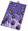
Importantly, single-vacancy and divacancy defects have now been individually probed within SiC using confocal microscopy ( Figure 4 ). This milestone demonstrates the viability of SiC as a platform for the manipulation of individual quantum systems in a wafer-scale semiconducting material. Somewhat surprisingly, the spin coherence times of both the vacancy and divacancy defects are longer than what might be naively expected, given previous observations of spins in diamond and the larger natural abundance of 29Si (4.7%) relative to 13C (1.1%). Reference Christle, Falk, Andrich, Klimov, Ul Hassan, Son, Janzén, Ohshima and Awschalom113 Computational techniques are being used here as well in an effort to explain this phenomenon. Reference Widmann, Lee, Rendler, Son, Fedder, Paik, Yang, Zhao, Yang, Booker, Denisenko, Jamali, Momenzadeh, Gerhardt, Ohshima, Gali, Janzén and Wrachtrup114

Figure 4. (a) Two-dimensional spatial scan of defect photoluminescence (PL) at the surface of a 4H-SiC sample. Light spots correspond to single or low numbers of defects. Circled spot in the center of the scan is a single divacancy of the (hh) type. The axis of this defect is aligned perpendicular to the page. (b) Rabi oscillations demonstrating quantum coherent control of single divacancy spins in 4H-SiC. Each panel shows data taken on a single isolated spin. Three of the four distinct defect forms are shown: (hh), (kk), and (kh). Reproduced with permission from Reference Reference Christle, Falk, Andrich, Klimov, Ul Hassan, Son, Janzén, Ohshima and Awschalom113. © 2015 Nature Publishing Group.
Conclusions
We have described the promise that quantum physics holds for future information technologies, as well as the role that semiconductor defect spins might play in the development of such device technologies. The NV center in diamond has proven to be a very versatile spin qubit, whose intense study over the past two decades has led to many exceptional discoveries regarding the physics of point defects, with an eye toward solid-state implementations of proposed groundbreaking quantum technologies in sensing, computation, and communication.
We have also described how these discoveries have led naturally to the search for deep-center defects with similar properties, but in host semiconductors that are amenable to microfabrication at the wafer scale. In this case, ab initio computational techniques represent a critical tool for discovering alternative materials systems with NV-like behavior. We have outlined the current state-of-the-art DFT-based computational methods for defect calculations, including the large-scale GW many-body perturbation theory calculation and the self-consistent hybrid functional calculation. We have also described how to model defects using the supercell method and a number of practical points to be considered during the computational search for potential spin qubits in nondiamond hosts.
First-principles calculations have played an integral role in the development of defect spin qubits in silicon carbide, most notably the silicon vacancy and divacancy defects. These defects are analogues of the diamond NV defect and exhibit a wide range of physical properties that, in many cases, complement those of the diamond NV defect with extended ranges of functionality.
Multiple studies of these defects have since laid the groundwork for continued exploration of defect spin physics in SiC as well as other semiconductors. Reference Rice, Ambwani, Bombeck, Thompson, Haugstad, Leighton and Crooker115–Reference Zwier, O’Shea, Onur and van der Wal117 With so many materials still largely unexplored, the future of defect-based quantum engineering is wide open.


