

When the Materials Research Society (MRS) was formed 40 years ago, it entered a very different social and technological landscape from that of today, and inevitably many of its priorities were different then. This article examines some selected areas of materials science that, while representing the breadth and scope of the discipline today, were on the whole either nascent or unguessed of four decades previously. Probably the most obvious, and arguably the most transformative, new field of science and technology to have emerged in the intervening time is information and communication technology: computer and cell-phone networks, wireless handheld electronics, new forms of electronic display, and the merging of electronic and photonic technologies. This is why three of the six topics considered here involve electronic materials. Meanwhile, advances in computation have made it possible to model materials with ever greater detail, precision, and verisimilitude than before, as acknowledged here by an examination of the challenges of computational materials science that spans many scales in size and time.
Materials science has long since burst the bounds of traditional engineering and moved into just about all areas of fundamental and applied science. One that will probably have the most profound impact on daily life is biomaterials: the development of new fabrics for medicine and bioengineering. Tissue engineering—the creation of new living materials, and the blending of the natural and synthetic—is perhaps the most remarkable example of this fusion.
The sixth topic here, materials for nuclear-waste management, is the exception in that it was very much an active field at the inception of MRS, and in fact represents one of the few topics to have remained on the agenda of the Society’s annual meetings from the outset until today. The fact that the materials issues (far less the social and political issues) have still not been solved is an indication of the difficulty of the challenge. Yet this was one of the first areas in which it was clear that materials science and engineering would be central to energy technologies.
These topics were chosen not just because of their intrinsic importance and, on the whole, their novelty, but because of their potential social impact. They all illustrate how the science is driven by societal demands and needs, and also how complex a matter it is to effect a transition from promising basic science to useful applications. In all cases, one can see a constant interplay between theory and empiricism, and examples of how advances in techniques and instrumentation can be at least as significant as advances in conceptual understanding. But what perhaps emerges most strikingly from these case histories is the degree to which advances depend on dialogue between different research communities. As polymer chemist Andrew Holmes of the University of Melbourne in Australia said, “[T]he big breakthroughs are coming from the interface of disciplines.” Interdisciplinarity has always been a strength of materials science—which in this sense at least was thus a harbinger of things to come.
Electronic materials: Oxides in electronics
In the march of information technology that has transformed daily life, it has tended to be semiconductors—the active materials for hosting and controlling the flow of current—that get all the attention. Yet the fabrication of ultrasmall electronic circuitry for logic processing and data storage would not have been possible without the other material constituents of the solid-state transistor, notably the insulating oxide dielectrics that isolate the charge-carrying components. In some ways it is these that have posed the greatest materials challenges. While the basic chemical nature of the semiconductors has changed rather little, the oxides that insulate transistor gates have been forced through a total rethink—and there may be more to come.
But it would be wrong to imagine that oxides in electronics are consigned to a passive role. One of the most profound discoveries in solid-state materials is the diversity of electronic behavior that can be instilled in oxides by controlling their crystal structure. Most notably, oxides were the unexpected materials for high-temperature superconductivity discovered in the mid-1980s. Some of these materials host the coupling of electronic to magnetic or optical degrees of freedom, for example, permitting sensitivity to magnetic fields that can be exploited in data readout. Oxides have become a playground for exploring new materials physics, with some important technological offshoots.
Closing the gate
In the early days of solid-state devices, nothing looked more convenient than silicon dioxide for use as a transistor gate insulator. The ease of making its oxide was actually one of the key attractions of silicon itself: it was never the best semiconductor, but was simple to oxidize, giving a sharp interface with few compromising vacancies. Silicon dioxide (SiO2) was “a fantastic material for processing,” according to electronic materials engineer John Robertson of Cambridge University in England.

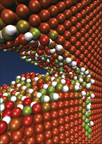
(a) A superlattice of barium titanate and strontium titanate, showing the atomic-scale precision with which the layer thickness and interfaces can be engineered. (b) The gates in microelectronic devices, such as this 16-Mbit memory chip, are insulated with oxides. Images: Ramamoorthy Ramesh, formerly at the University of California–Berkeley.
However, for the standard complementary metal oxide semiconductor (CMOS) transistor of microelectronic circuitry, SiO2 had its limitations. When the insulating layers became thinner than about 1.2 nm (about five atomic layers) as miniaturization reached the so-called 45-nm node, they were no longer perfectly insulating: they leaked current, limiting the amount of charge that devices could store. And for every further angstrom of thinning, the leakage increased tenfold because of quantum tunneling. Silica needed to be replaced with another material with a higher dielectric constant. By the start of the new millennium this problem was urgent.
One of the best candidates to emerge at that time was hafnium dioxide (HfO2), with a dielectric constant about five times that of SiO2. But in other ways it wasn’t ideal at all. It was a fast ionic (oxide) conductor, and in contact with highly doped silicon (the gate metal for transistors) it incurred oxide vacancies which meant, in effect, that the devices couldn’t be wholly turned off. So to make the new oxide work, in the early 2000s Intel elected to transform the whole manufacturing process, using a real metal (not disclosed) for the gate and changing the fabrication procedure so that gate fabrication comes last. “This meant billions of dollars of investment,” said Robertson.
Intel began shipping transistors with the new gate oxide in late 2007, after which most other microelectronics companies followed suit. Success—about which many were initially pessimistic—depended also on the advent of new fabrication methods, such as atomic-layer deposition. Now HfO2 is the industry standard—thanks to materials scientists, “all the issues are sorted,” according to Ramamoorthy Ramesh of the Oak Ridge National Laboratory—yet remarkably, the consumer end of the market didn’t even notice how profoundly the materials basis of the industry had been transformed. But Robertson warns that the thickness of the gate oxide is now already getting small enough to become problematic again as the rollout of 15-nm technology looms. He said that this time a complete change of device architecture might be called for, with the conducting channels being wrapped around with the gate and oxide on three sides, offering greater current control at lower voltages.
Oxide memories
If gate oxides are subjected to too high a voltage, they can fail catastrophically in the process of dielectric breakdown, where passage of a current permanently disrupts the material’s crystal structure. But this breakdown doesn’t have to be destructive and irreversible. Under some conditions, a conduction pathway can appear and then vanish again, for example by the migration of defects in the crystal, giving rise to so-called soft breakdown. The reversibility means that this process can furnish a memory device, and several companies are working to develop this effect into resistive random-access memories or ReRAMs. A variety of materials are being considered, but oxides look to be some of the most promising—including oxygen-deficient HfO2 and even silica—because their relatively mobile oxygen vacancies may form the conductive track.
The use of functional oxides for data storage is more advanced in ferroelectric random-access memories (FeRAMs), which exploit the property of ferroelectricity displayed by several compounds, including barium titanate, bismuth ferrite, and lead zirconate titanate (PZT). These oxides have been used for decades as smart materials in piezoelectric sensors and actuators. In memories, their attraction is that switching of ferroelectric polarization can be sustained without an applied voltage. As a result, FeRAMs (like ReRAMs) could offer “nonvolatile” random-access memories, in which data unsaved to a hard drive is not lost during a power failure or computer crash. “Once this new kind of memory hits the market, it will make a huge difference,” said Ramesh.
Nonvolatile memory is already achieved using flash memory, in which the cells are a kind of transistor switched by a process of quantum tunneling of electrons through a very thin dielectric layer. But the tunneling barrier gets weaker after many thousands of switching events, so the memory elements become leaky. A typical dynamical RAM, however, might undergo many trillions of write and read events in its lifetime.
Another problem with most current RAM devices, whether volatile or not, is that readout is destructive: it erases the data. Ramesh and his co-workers recently reported a bismuth ferrite FeRAM in which the readout is optical and nondestructive, making use of a photovoltaic current induced by a laser pulse. As with many of these new candidate nonvolatile RAMs, however, one big question is whether the memory cells can be made small enough to compete with flash and magnetic storage: commercial FeRAMs, marketed by Texas Instruments and Fujitsu, have elements a whopping 350 nm across.
Whether ReRAM, FeRAM, or something else will win out as the “universal memory” remains to be seen. The Sony PlayStation® used some early FeRAMs, for example, but they were soon overtaken by flash. “We’ve already got tons of memory,” said Robertson. “We don’t need another bad one.”
Sometimes it’s the physics rather than the applications that drives interest in functional oxides. It was discovered over half a century ago that the resistance of mixed-valence perovskite oxides such as lanthanum strontium manganite can be altered dramatically by magnetic fields thanks to coupling between the spins of the magnetic atoms (here manganese) and the electrons. This effect, called colossal magnetoresistance, could potentially provide a magnetic readout technology—but it first needs to operate at much lower magnetic fields. “The science is fascinating,” said Ramesh—but the practical value is still unclear.
Such oxide materials are great for doing science, said Robertson, but it’s very hard to use them to make a device that works. But he feels that the very conservativeness of the traditional materials base in electronics makes it a good time to be working on such materials: there are still lots of new possibilities and opportunities, even if inevitably not all will bear fruit. “The evolution from science to technology is always uncertain,” said Ramesh. “The question is, how do you turn knowledge into value?”
Electronic materials: Organic electronics
Perhaps the first rule of any new electronics technology should be don’t try to compete with silicon. It’s not that silicon integrated circuits can’t be bettered, but rather, the technology has been so refined, optimized, and streamlined that any alternative will need far more than just one or two putative advantages. This dictum is well illustrated by organic electronics, which is now a thriving, if still fledgling, business because it has been able to find complementary niches—to reach parts that silicon can’t.
For example, organic electronics looks likely to make an impact in biomedicine, where circuits that are flexible, biocompatible, and even biodegradable can literally conform to the demands of the application. For display technologies, silicon was never well suited anyway, and organic light-emitting devices (LEDs) are entering a field already geared to the organic media of liquid crystals. Where cheapness and robustness matter more than performance—for example, in solar cells for rural settings of developing countries—organic devices are making inroads. The key is to complement, not compete with, silicon logic.
Delayed development
Forty years ago, no one imagined using polymers and other organics in electronic applications. The first conducting polymer, polyacetylene (doped with impurities), was still a serendipitous mystery material sitting in the laboratory of Hideki Shirakawa at the Tokyo Institute of Technology. The field only truly took off after switching its focus from “polymer metals” to polymer semiconductors, leading to the synthesis of polymer-based transistors and light-emitting diodes at the end of the 1980s. The award of the 2000 Nobel Prize in chemistry to Shirakawa, along with conducting-polymer pioneers Alan Heeger of the University of California–Santa Barbara and Alan MacDiarmid of the University of Pennsylvania, was a recognition that organic electronics had finally arrived.
One key to this success was the possibility of using chemical synthesis to diversify and fine-tune the materials. “We can utilize the power of chemistry to change the molecular structure in ways that impact the macroscopic properties,” said chemical engineer Zhenan Bao of Stanford University.
For example, conducting polymers such as poly(para-phenylene vinylene)—used by physicist Richard Friend of the University of Cambridge, chemist Andrew Holmes then at Cambridge, and their collaborators to make some of the first “plastic LEDs”—didn’t need doping and were chemically stable, and their emission color could be altered by tinkering with the molecular structure. Some of this tuning of color drew on knowledge developed long ago in the dye industry, involving the adjustment of the gap between the molecules’ highest energy-occupied and lowest-unoccupied electron orbitals. “The first challenge was getting away from yellow-green to red and then finally to blue,” said Holmes.
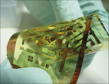
Flexible electronic circuit made from organic conductors. Image: Zhenan Bao, Stanford University.
Another vital step in the 1980s, due in particular to Heeger and Fred Wudl at the University of California–Los Angeles, was to develop polymers that were solution-processable, so that simple “wet chemistry” could be used to synthesize thin films, rather than having to deposit the monomers and then polymerize in situ. “Until that time all of these polymers were intractable—they couldn’t be dissolved or properly characterized,” said Olle Inganäs, a specialist in organic electronics at Linköping University in Sweden. Solubility made it possible to produce well-defined thin films, and to adjust their parameters. Bao said, “We can use side chains not only to solubilize the polymers but also to control the distance between them, and thereby their interactions and the charge transport through them.”
A significant development for light-emissive devices was to harness all the energy of the excited state. Typically for these conjugated organic molecules, three-quarters of the excitation energy went into a state that didn’t emit but was ultimately squandered as dissipated heat. Around 2001, Stephen Forrest and Mark Thompson at Princeton University found a way to liberate this energy in small organic molecules through phosphorescence, greatly boosting the efficiency. “That was a big breakthrough,” said Holmes.
In the early days, the potential of conducting polymers and other organic electronic materials was stymied partly by their instability. “The issue of lifetimes came up as people really started to think about manufacturing practical devices,” said Holmes. But this is, on the whole, no longer a problem: organic LEDs (OLEDs) are now lasting for 100,000 hours. “We can soak our polymer transistors in seawater for several months and they are still functional,” said Bao.
Molecular control
Over the years, some consensus has emerged about the best materials for each application of organic electronics. For OLEDs, most current polymers have polyfluorene (two benzene rings linked by a five-membered ring) or carbazole (the same, with a nitrogen atom in the linking ring) as the building block. “This is robust, can be made solution-processable, and can be cross-coupled to other units,” Holmes said. “For transistors, thiophene [cyclic C4H4S] still hogs the road,” he said.
But by no means does all organic electronics use polymers. Most of the research on light emission, for example, currently uses small organic molecules instead, which are typically deposited by evaporation. With small molecules, it is possible to make very precise nanoscale devices with sharp interfaces, and they are purified in the evaporation step. “They have an intrinsic superiority if you want to make very complex structures,” said Inganäs—such as LEDs using very thin multilayers of several different emissive materials. “This debate is still going on,” said Holmes. “The preference has been to go for small molecules for early commercialization, but polymers haven’t been ruled out.”
One of the major challenges in improving the electronic and optical performance of all organics is to control the ways that the molecules pack together: their morphology. “Morphology control has improved charge-carrier mobilities a lot, but predictability is the great unsolved area,” said Holmes. “It’s still pretty empirical.” The material morphology can also be hard to reproduce—a crucial requirement for manufacturing.
Making headway in solving this problem with morphology demands better fundamental understanding of how molecules arrange themselves, and how this self-assembly can be harnessed and directed. “We need rational design to significantly move the field forward,” said Bao. “The time is right: we have lots of computer power, lots of fundamental knowledge, and much better tools for analyzing structure. Computational theory can now make a significant contribution to predicting properties. In the next twenty years, I think this field will move much faster because of these things.”
On the market
Displays, transistors, and solar cells are currently the three main areas of organic electronics. OLEDs are already being used in commercial products: Samsung’s Galaxy S cell phones, for example, use emissive displays rather than backlit liquid-crystal devices, and Samsung, LG, and Panasonic have developed OLED flat-screen televisions—the first two likely use small molecules for the emissive layer, the latter a conjugated polymer (such details are generally kept secret and often depend on hearsay).
Their low cost should open up new markets, for example in the development of organic solar cells that might provide “off-grid” power alternatives to kerosene burning in developing countries. Polymer solar cells can now achieve energy-conversion efficiencies 8.5–9%, comparable to off-the-shelf silicon cells. Inganäs, whose own work focuses especially on photovoltaic applications, said that it is with such large-area devices that the potentially cheap processing of organic materials could win out over inorganics, even if their performance is not quite as good. He sees light-emission for illumination (rather than displays) as another such area where low cost could make the difference. In both of these cases, the flexibility of polymers is also important, for example to make foldable solar cells.
Organic electronics is already demonstrating its potential to enter areas into which silicon technology has barely even considered venturing. For example, chemist Timothy Swager at the Massachusetts Institute of Technology (MIT) has exploited the fact that some organic molecules will form charge-transfer complexes with conjugated polymers to develop a highly sensitive chemical sensor for explosives such as TNT. The nitro aromatics in such explosives will engage in a donor–acceptor interaction that quenches the emission of the donor polymer, so that its light will dim slightly if such compounds are present. This forms the basis of a commercial device called Fido—an allusion to the fact that its sensitivity can equal that of a sniffer dog’s nose—that is being used to detect landmines and traces of explosives on clothing and vehicles in military field operations, thereby saving lives.
“If I ever saw a great use for organic electronic devices, it is at the interface with biological systems,” said Inganäs. An advantage here, he said, is the ability to match the mechanical properties of the material to those of living tissues. Bao has used a variety of organic materials, including carbon nanotubes, self-healing supramolecular polymers, and organic transistors, to develop touch-sensitive “electronic skin,” which she said might find applications in prostheses, robotics, and sensing of health and medical conditions. Placed on the steering wheel of an automobile, an electronic skin could continuously monitor the driver’s alertness—whether he or she is still gripping the wheel firmly.
A particularly dramatic example of such medical applications is the effort to interface conducting polymers with the human nervous system, currently being pursued by polymer chemist Gordon Wallace of the University of Wollongong in Australia. “I think that is genius stuff: the interface with human organs is very important,” said Holmes. Meanwhile, John Rogers at the University of Illinois at Urbana-Champaign has created stretchable, biodegradable circuits that can be placed directly on the skin and even on the brain. He is developing a skullcap with polymer sensors that could detect concussive impacts to the head of a footballer, and will signal that information through an OLED “traffic-light” system attached to the back of the player’s neck.

Samsung’s prototype of a flexible organic light-emitting diode display called “YOUM.” Courtesy Samsung Electronics Co., Ltd.
Bao is hesitant to rule out the possibility that organics might even prove genuinely competitive on silicon’s home turf. “We still don’t know what is the ultimate electronic conducting ability of these polymers,” she said—for example, if conduction can be made continuous within a single chain from one end of a device to the other, “in theory it could be very fast.” That alone won’t vanquish silicon—but it might open up yet other fields for organics.
Electronic materials: Carbon nanostructures
When the cage-like carbon clusters called fullerenes—most notably the beautifully symmetrical C60—were discovered in 1985 and then mass-produced in the early 1990s, they seemed at first to be primarily of interest to chemists. But while C60’s principal discoverers Harry Kroto, Richard Smalley, and Robert Curl were awarded the 1996 Nobel Prize in chemistry, the subsequent experimental identification of carbon nanotubes (CNTs) by Japanese microscopist Sumio Iijima in 1991 shifted attention toward the electronic properties of such giant carbon molecules, which proved capable of acting as conducting nanowires. It soon became clear that CNTs and fullerenes are but representatives of an entire menagerie of carbon nanostructures, which now includes nanoporous carbon foams, cones, and “onions,” and the graphitic carbon sheets called graph-ene: the thinnest material yet found, and second in strength only to diamond.
Some researchers, such as Rodney Ruoff of the University of Texas at Austin, believe that the mechanical properties—strength, flexibility, and stiffness—of these nanoscale carbon materials will turn out to be one of their most valuable attributes, making them a nanotechnological evolution of traditional carbon fibers. But others are convinced that carbon will enter, and perhaps eventually dominate, the electronics market. “There’s no reason for it not to replace silicon,” said physicist Walt de Heer of the Georgia Institute of Technology in Atlanta. “I fully expect this will happen, but probably not in my lifetime—it will take decades.”
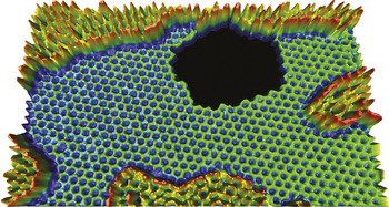
A graphene sheet imaged with the transmission electron microscope, showing a hole around which rearrangements of individual atoms can be monitored in real time. The higher regions are additional layers of less structured carbon. Courtesy Zettl Research Group, Lawrence Berkeley National Laboratory and University of California–Berkeley.
Balls, wires, sheets
Like many others now working on carbon nanostructures, both de Heer and Ruoff entered the field from a background in research on small atomic clusters. “One fascinating thing about carbon is that its valence is saturated even in tiny structures,” said Ruoff. “In contrast, many elements, when we shrink their size, are highly reactive.”
Carbon achieves this because it can form sheets, curved shells, and tubes in which each atom is bonded to three neighbors, in general forming hexagonal rings, like those in graphite. The delocalized bonding creates potentially mobile electrons. In 1998, de Heer and co-workers found that the electrons in CNTs can travel ballistically—without any scattering—so that their mobility is very high.
In comparison to fullerenes, CNTs seemed promising for electronics because they are extended in one direction, making them capable of transporting electrons over micron scales. But even though CNTs were wired up with metal contacts to make transistors in the late 1990s, there were big obstacles to turning such devices into a useful technology.
For one thing, standard methods of making CNTs by growth from carbon vapor on catalytic metal nanoparticles tend to produce a mixture of tube diameters and atomic structures, some of which are metallic and some semiconducting—just as was first predicted in 1992 by the pioneer of nanostructured carbon Mildred Dresselhaus at MIT. For a transistor one wants only the latter. The challenge of synthesizing just one kind of tube, or separating a mixture, for large-scale production still remains. But Ruoff is cautiously optimistic, saying “there’s been good progress along that front.” For example, Yan Li and her colleagues at Peking University have used catalytic growth to make aligned CNT arrays that are at least 95% semiconducting.
Yet whether CNTs will ever really make good channels for transistors is unclear. “There are a lot of reasons why you simply can’t integrate CNTs into electronics, basically because of interface problems,” said de Heer. “If you want to wire up a CNT you ultimately are forced to put metal leads on it. Those leads are terribly fragile, and the interfaces are highly resistive, making every property you get in the nanotube completely irrelevant.” Yet despite such challenges, the development of imperfection-tolerant circuit designs have kept hopes for CNTs alive, and very recently a team at Stanford University demonstrated a simple computer made entirely from nanotube transistors.
Concerns about the problems of CNT electronics prompted de Heer in 2001 to turn instead to graphene. “I decided that if CNTs have this ballistic property then that’s probably a property of graphite itself,” he said. “It was very well known since the mid-1970s that silicon carbide grew these fantastic graph-ene layers on it. Silicon carbide is a known electronic material, so I thought it would be an ideal platform to build graphene nanostructures that hopefully can be wired together with this ballistic property.”
Graphene research didn’t take off on a global scale, however, until 2004, when Andre Geim, Kostya Novoselov, and their co-workers at Manchester University in England found that the sheets could be made cheaply and easily by using Scotch tape to peel away flakes of graphite atomic layer by layer, ultimately perhaps leaving just a single layer. This approach had been used before for other layered materials, but it caught the imagination and made graph-ene research accessible to all.
It was, however, Geim and Novoselov’s work on the physics of the carbon sheets, not their Scotch-tape strategy, that won them the Nobel Prize in physics in 2010. They used their peeled-back samples to show that graph-ene has some very exotic electronic properties indeed. Confined to two dimensions in the hexagonal carbon lattice, the electrons move collectively as “quasiparticles” with a zero effective mass, making them behave like ordinary electrons traveling close to the speed of light. This means that graphene can host strange quantum mechanical behavior, such as electron tunneling through energy barriers no matter how high and wide they are. Their work was “a huge contribution to fundamental physics,” according to Andrea Ferrari, director of the Cambridge Graphene Centre at Cambridge University.
Mind the gap
Whether graphene is a good substrate for practical electronics is another matter. Inconveniently, the electronic structure has no bandgap: electrons need no extra energy to move from the valence to the conduction band. So it isn’t a true semiconductor at all: if it is used to make a transistor, it can’t be switched off.
Researchers are therefore looking for ways to open a bandgap. Calculations suggested that this should happen in graphene nanoribbons because of the influence of edges. But although experiments seem to bear that out, the ribbons don’t have a true bandgap but rather a so-called mobility gap that arises because of scattering from defects. “If you use electron beams for patterning graph-ene into nanoribbons, it’s like tearing paper,” de Heer said. “You get rough edges and a whole bunch of other stuff. That means it is useless for electronics.”
To be genuinely useful, graphene nanostructures will therefore probably need atomically smooth edges. That’s why there is now a lot of interest in bottom-up synthesis: polymerizing polycyclic aromatic molecules into predefined graphene nanoribbon patterns. De Heer, meanwhile, has found that at high temperatures the graphene nanostructures that he carves out on silicon carbide can be annealed to remove edge defects. But even then the bandgaps might be rather small, which means that electrons would easily be thermally excited into the conduction band and so the devices could be noisy.
A big question remains about the best way to make graphene. Despite its convenience and cheapness for laboratory research, the Scotch-tape method seems unlikely to be of value for applications—the materials it makes are too full of impurities and defects, said de Heer. Geim concurs, saying, “I can’t imagine Intel using our method.” Ferrari said there is typically a big gap between the theoretical properties of an ideal material and the real properties of products that can actually be made.
Ruoff said that chemical exfoliation methods, which separate graphite sheets in solution, should be valuable for some two-dimensional materials, but admits that making pristine graphene flakes this way has not yet been achieved in a scalable manner. Besides, he notes that the semiconductor industry is already geared up for using chemical vapor deposition methods to make their thin films. However, Ferrari and his colleagues in Cambridge have developed a technique for making transistors and conductive patterns using exfoliated graphene deposited by inkjet printing.
But cheapness of the material or processing needn’t be the main objective. “There’s not a single industrialist who will tell you that’s their primary motive for choosing a material,” de Heer said. He argues that, while his silicon-carbide route is more expensive, it isn’t prohibitively so. “If this electronics materializes, in the beginning it is not going to be cheap,” said de Heer. “But that’s how technology goes.”
The road for carbon
Nevertheless, big things are predicted for graphene. The European Commission has just approved a €1 billion (USD$1.3 billion) 10-year project called the Graphene Flagship for developing technologies using the material, which might range from electronics and optoelectronics to displays and sensors. Ferrari, who leads the team developing the project’s science and technology roadmap, said it isn’t focusing on graphene alone but also investigating other layered two-dimensional materials such as boron nitride.
He stresses that the first electronic applications won’t be in areas that compete with silicon. “Graphene has to go where there isn’t an alternative,” he said—such as conducting inks, stretchable circuits, and conductive composite materials, and perhaps later into optoelectronics. A small start-up company called Novalia in the United Kingdom, for example, is already using graphene-based inks to make wires for an interactive, touch-sensitive printed poster that can communicate wirelessly and generate drum-kit sounds through vibrations of the paper itself. Partly because it is cheap, said Ferrari, graphene “could put functionality into objects that don’t usually have it.”
At first, then, graphene devices need to play to its strengths. “We are not out to compete with silicon, but to extend it,” agrees de Heer. “We’re looking at high-end, not necessarily cheap, electronics that goes beyond anything that’s possible with silicon.” One such niche is in high-frequency devices for optoelectronic telecommunications applications, which would benefit both from graphene’s high mobility and its high thermal conductivity and robustness, which helps to dissipate the heat generated by rapid switching. “Within a relatively short time, I think we are going to be producing electronics working at terahertz frequencies,” said de Heer—several orders of magnitude faster than current silicon devices. Ruoff also sees potential for completely different electronic roles, such as electrodes in batteries and fuel cells. His group recently showed how to make nanoporous graphene that can outperform the standard activated carbons in such devices.
But perhaps the real killer app for carbon nanostructures has yet to be identified. “There’s been a wonderful streak of serendipity in this field—scientists in the lab thinking one thing will happen, and quite a different thing does happen,” said Ruoff. “I think that will continue with carbon, because there’s such a plethora of different bonding configurations, and there’s still a lot of really exciting directions to go.”
Multiscale materials modeling
“If we are going to set out to invent entirely new materials,” wrote the engineer Jim Gordon in the second edition of his classic book The New Science of Strong Materials, published three years after MRS was created in 1973, “then we had better watch our step because the requirements for any really successful material are likely to be very complex indeed.” Much of Gordon’s book was dedicated to explaining mechanisms of ductility, cracking and failure in metals, ceramics, and composites, and it’s safe to assume he already had an inkling of where, in such cases, much of that complexity comes from. Cracks, as Gordon showed, begin with the breaking of bonds between atoms, but may end with the collapse of bridges. How can one hope to understand a process that spans perhaps 10 orders of magnitude in size?
The development of computer methods for modeling materials systems at the atomic scale, in its infancy in Gordon’s day, has now reached the level where some methods can handle millions of atoms, and continues to grow as computer power expands. But there is no prospect that this bottom-up approach will encompass all the scales that a materials engineer might need to consider, not only because the numbers are so vast but because more atoms don’t necessarily mean more insight. “A cubic micron of material contains about a trillion atoms, so there’s no way to treat that atomistically,” said Christopher Wolverton of Northwestern University in Evanston, Ill., who works on computational materials science.
A simulation of how accumulation of interstitial hydrogen atoms (white) around the tip of a crack in iron (other colors, indicating potential energy) cause embrittlement. Courtesy W.A. Curtin.
So for aiming to understand and perhaps even to design materials from first principles, computational methods are needed that can span diverse scales in space and time. “The challenge is to connect the chemistry and microstructure to all the macroscopic behavior that the materials need to have, such as strength, toughness, stiffness, fatigue resistance, creep resistance, and corrosion resistance,” said Bill Curtin, director of the Institute of Mechanical Engineering at the École Polytechnique Fédérale de Lausanne, Switzerland. “You’re always balancing the material to encompass all of these things in one way or another.”
Shaking hands in metals
Multiscale materials modeling should help to confer an element of predictability on what was previously a matter of discovery by trial and error. This is true, for example, in the area of metal alloy engineering, which has already so benefited from the insights offered by simulation that it is becoming possible to talk about “first principles metallurgy.”
“The macroscopic behavior of a metal doesn’t just depend on what goes on at the atomistic scale, but also on the mesoscopic scale of dislocations and how that is influenced by microstructure,” said Curtin. “In metals you have to worry about plastic flow at scales of tens or hundreds of microns. It’s a challenge to get the whole picture and be quantitative about it.”
One of the key requirements for the complex, multicomponent formulations of some high-value alloys today is to understand their phase stability: whether the constituents will mix or precipitate into distinct microdomains. In industry these formulations can be extremely complex, not least because the materials aren’t necessarily purified. “A typical engine-block alloy has about twelve elements, including a lot of stuff picked up in recycling, and the companies aren’t going to change that,” said Wolverton.
Phase precipitation in these alloys can create domains typically several hundreds of nanometers across, which can act as obstacles for dislocation motion and thereby contribute to hardening and embrittlement. A common approach to understanding precipitation uses a technique of computational thermodynamics called CALPHAD (Calculation of Phase Diagrams). “This is reliant on giant databases of thermodynamic functions,” said Wolverton. “It’s very successful, but if the thermodynamic functions are not in the databases then you’re out of luck.”
While working at Ford, Wolverton and his colleagues were often faced with that situation because they were interested in metastable phases, which the databases don’t heed. He was able to calculate these missing thermodynamic functions using first-principles density functional theory, which doesn’t care whether the phase modeled is absolutely stable. In this case, as Curtin said, “the thermodynamics can be more or less taken down to some sort of unit-cell scale.”
This approach of performing calculations at one scale to derive the necessary inputs for the next scale-up is called “parameter-passing”—Zi-Kui Liu of The Pennsylvania State University thinks of it as a “handshake” between scales. “We try to pick out only what’s important at each scale,” he said. The aim is to create a continuum model appropriate to a given scale that integrates information at finer scales and is practically useful to scientists and engineers.
Yet this handshake approach isn’t always possible, because the interactions between scales are not just one-way: what happens on the mesoscale might alter the situation on the atomic scale, for example. In such cases one might need to resort to so-called concurrent modeling, which entails simultaneously solving all the appropriate equations in the respective domains. In this picture, said Wolverton, “a single calculation would contain all of these different length scales within it.” Certain parts of the problem can be handled at a finer scale, while others ignore the details. For example, one might model an atomistic dislocation core embedded in a medium that just cares about the long-ranged elastic strain field the core induces.
To find ways of linking all the scales of the problem dynamically is a tremendously challenging task both computationally and conceptually. But as Curtin explains, sometimes “there are certain things that save you. For example, if you want to follow a crack tip, you just need to know the stress intensity there. So even though things talk back and forth, there are ways to separate them.” That, he adds, is why computational materials is not just all about simulation: “we need theory behind it, to tell us when and how to separate scales and when they have to talk to one another.”
Softer solutions
The existence of multiscale, hierarchical structure has been long known in the living world, particularly in soft and composite materials such as silk, bone, and wood. Cells themselves can be envisioned as complex functional materials of this sort. And in polymer science, it has been recognized that mechanical properties may depend on the formation of microcrystallites, which in turn is influenced by the packing of the chain molecules.
Polymer scientists commonly apply a “coarse-graining” approach in which many-atom chunks of the molecules are represented as single particles that interact in a way that approximates all the individual interatomic forces, perhaps using potential functions derived from higher resolution simulations. Christine Peter at the Max Planck Institute for Polymer Research in Mainz, Germany, uses such approaches to look at the self-assembly of biopolymers that serve as templates to create ordered inorganic materials. The challenge is to find some way of carrying the specific chemical variations up to the coarse-grained level, rather than just ending up with generic “blobs.”
Here too problems of concurrent processes at different scales, and transferability between scales raise their head. “We have learned a lot about how to make coarse-grained models for a given state point, but during the formation of such a system the situation changes over large scales in time and space, so your coarse-grained model would in principle need to adapt continuously to the changes,” Peter said. At root, she explains, the problem here is that the model has to cope with out-of-equilibrium situations—which is “one of the major issues of soft-matter modeling.” Also, coarse-graining smooths the landscape of energy states for different configurations in a way that speeds up the dynamics artificially—which can be an advantage, but also raises the problem that not all dynamic processes might scale up in the same way, so the time scales get distorted. These are concerns that apply not just to soft matter but to any attempts to model self-assembly and growth in materials synthesis.
Computational design
Curtin thinks it will ultimately become possible to design materials properties from first principles. “It’s already happening for some properties, such as phase stability,” he said. But designing toughness or yield strength, or modeling fracture and fatigue, will be another matter entirely.
Liu thinks, however, that the aim will never be just to predict a material from the drawing board—experiments will always be needed to guide the computations. “Computation will just narrow the options, it’ll never completely predict,” he said. “We can’t compute everything.” In particular, computation could overlook outliers—materials with anomalous behavior, which is often where discovery comes from. As a result, Liu wants faster experiments as much as faster computers—it’s not a case of computation versus experiment, he said.

An extrinsic stacking fault in hexagonally closed-packed magnesium. Defects at the atomic scale, which are revealed in the electronic structure shown here, affect the macroscopic mechanical properties such as the elastic and plastic deformation. Credit: W.Y. Wang and Z.K. Liu: private communication.
“Computer power is fantastic and essential, but you really need concepts and mechanisms to interpret and generalize the results,” Curtin agrees. What’s needed, he said, is “the combination of this computer power in the hands of creative scientists who can perform the right computations, build the advanced algorithms, and develop the new conceptual and mechanistic models to interpret computational results.”
Peter agrees that in her field too, modeling might be more of an analytical than a predictive tool. “By reducing the number of degrees of freedom in coarse-graining, you have a way of learning the relevant aspects of the system.” Besides, she said, “let’s be honest, doing the experiment is often faster [than predicting it]. What we can provide is a microscopic interpretation that is very often missing.”
More than bigger computers, said Curtin, what the field needs is multiscale thinking: to educate students to think about knowledge across scales. “Fifteen or so years ago there weren’t applied mechanics people worrying about atoms, while physicists weren’t worrying about dislocation networks. Now these fields are merging somewhere in the middle.” He sees the emergence of the individual researcher “who is sufficiently knowledgeable about methods, mechanisms, and concepts across scales to execute at one scale and translate to other scales. This merging of areas of condensed matter and statistical physics, materials science, and applied mechanics, within each researcher is incredibly important.”
Materials in tissue engineering
When in the mid-1980s pediatric surgeon Joseph Vacanti of the Massachusetts General Hospital (MGH) became frustrated that his efforts to save children’s lives through transplants were hindered by a shortage of organs, the idea of growing them to order would have struck most people as science fiction. Three decades later it is becoming a reality, and Vacanti is extremely upbeat about the prospects. “With every year I see more hope even for the most difficult problems of tissue regeneration, such as brain repair after strokes or spinal-column damage,” he said.
Although in 1985, Vacanti performed a successful liver transplant on a child, one of the few options available for obtaining child livers was to trim adult livers, which was fraught with difficulty. “It occurred to me that if we could build liver tissue, we could transplant on demand,” said Vacanti. “The question became, how?”
Vacanti knew of work in the 1970s in which artificial skin was grown from cultured cells on a scaffold of natural polymers. He turned to his friend Robert Langer, a chemical engineer at the Massachusetts Institute of Technology, and they began to look for ways of culturing liver cells on a polymer substrate, using materials similar to the earlier work that were already approved for human use. “We combined materials science and engineering with biological and clinical science,” Vacanti said. Cells will survive in culture if adequately supplied with nutrients and wastes are removed. The issue is how to enable this in a three-dimensional structure. Inspired by the branching shape of seaweed, Vacanti suggested that they use an open, porous structure as the scaffold. “It soon became apparent that we could extend the idea to all tissues,” he said.
But Vacanti warns against under-estimating the challenges involved even with what might seem like relatively simple tissues. He and others engineered artificial cartilage in the mid-1990s, which might for example be used to fabricate ears. But these still haven’t been used on humans because the wound-healing process after transplantation is complicated: the synthetic cartilage tends to be resorbed over time, causing the tissue to deform. “It’s taken a lot of work to prevent this,” said Vacanti. “This is difficult science.”
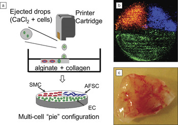
(a) Schematic drawing of a three-dimensional (3D) bioprinting method to fabricate multicell tissue constructs of canine smooth muscle cells (SMCs), human amniotic fluid-derived stem cells (AFSCs), and bovine aortic endothelial cells (ECs); (b) fluorescence microscopic top view of the printed complete 3D multicell “pie” construct before implantation, where SMCs appear red, AFSCs appear blue, and ECs appear green; (c) tissue vascularization of the ECs printed cell construct eight weeks after implantation. This work demonstrates the feasibility of fabricating complex heterogeneous tissue constructs containing multiple cell types using inkjet printing technology. Reproduced with permission from Biomaterials 34, 130 (January 2013), DOI: 10.1016/j.biomaterials.2012.09.035. © 2013 Elsevier B.V.
Giving the right signals
A key question is how much cultured cells can be trusted to do things on their own, and how much they need to be guided. Cells communicate as they grow, migrate and cohere into tissues, and they can to some extent take care of growing their own vascular system for blood supply. They already contain gene programs for shaping and forming tissues during an organism’s growth, and for wound healing. But they may still need scaffolds to help them find the right form. That’s why some polymer scaffolds are designed to be “smart”: to send guiding signals to the cells, often in the form of chemical agents bound to their surface by covalent linkages. For example, biodegradable, fibrous alginate biopolymer scaffolds have been prepared with cell-adhesion peptides attached that regulate cell attachment and spreading, while functionalizing these scaffolds with heparin promotes the attachment of heparin-binding growth factors that can assist wound healing.
Many efforts in tissue engineering now make use of stem cells, which have a capacity (called pluripotency) to grow into any tissue type. Most enticing of all is the possibility of using stem cells created for the purpose from the recipient’s own tissues. Perhaps the most dramatic recent discovery in stem-cell science has been that mature differentiated cells such as skin can be returned to a pluripotent state by chemical means. Using such induced pluripotent stem (IPS) cells, just about any organ type could in principle be grown from an adult’s own cells. Very recently this sort of reprogramming of mature cells was achieved even in live mice.
Tissue engineering with stem cells is still relatively new, but it holds enormous promise: organs containing several cell types, such as vascular cells, bile and liver cells in a liver, might all be cultured from the same stem cells, which differentiate into specific tissues when given the right chemical and environmental cues. Various small peptides attached to polymer scaffolds have been shown, for example, to regulate the viability, growth, and differentiation of a certain class of stem cells that can become osteoblasts (bone-forming cells), connective tissue, and other cell types for bone regeneration.
Mechanical forces can also affect growth and cell fate; for example, stresses applied to bone scaffolds in vitro may induce the formation of osteoblasts or smooth muscle cells, depending on how the loading is applied. Reproducing the forces in cell culture that such tissues experience in vivo can help to generate the right arrangements and balance of bone, ligament, and so forth in regrown tissue. The elasticity of the scaffold is also crucial: some stem cells produce neurons on soft surfaces, muscle on stiffer ones, and bone on rigid ones. Cells also “talk to” and affect one another, for example by releasing growth factors and hormones, and so it can be important to seed a scaffold with the right distribution of cell types.
Controlling these cues places big demands on the scaffold’s architecture. “There are multiple cues that you have to think about when designing a material,” said laryngologist Martin Birchall of University College London in England, who has developed tissue-engineered windpipes for human transplantation. “The micro- and nano-patterning of a surface you put a cell on will critically inform what it decides to do.” In one recent example by Eben Alsberg of Case Western Reserve University in Ohio, an alginate hydrogel was micropatterned by photo-cross-linking through a mask, and the pattern size was found to regulate the cell proliferation rate and to affect the balance of differentiation into bone-forming and cartilage cells. Patterning the adhesive properties of a rigid cell support has been shown to control the differentiation of stem cells into bone or fat cells.
The matrix, rebooted
It’s because of such architectural subtleties that advances in three-dimensional (3D) printing techniques should be a boon to tissue engineers. These methods, which build complex shapes layer by layer using polymerizable materials delivered through a fine nozzle, can be used to construct the most convoluted and heterogeneous structures, or to reproduce exactly the shape of the organ or tissue that needs replacing. This approach was used this year by researchers at the University of Michigan to tailor a purely synthetic polymer sleeve that could prevent a malformed section of an infant’s trachea from collapsing and blocking his airway. Birchall explains that “you can take a CT scan of a patient pre-operatively and use 3D printing to produce something that is exactly the right size and shape.” This approach is already used for making bone substitutes for craniofacial surgery.
And it’s not just the scaffold that could be made this way. Printing methods have now been demonstrated with living cells as the “ink,” protected within droplets of soft hydrogel, making it conceivable to “print” new organs. “3D printing will make a huge difference to the field,” said Vacanti.
Another option is to forgo synthetic scaffolds entirely and use the robust extracellular matrix of an actual donor organ instead. Here, chemical methods involving detergents and enzymes are used to wash away all the donor cells, leaving just the “decellularized” organ, on which the recipient’s cells are then grown. Because of the removal of cells, animal organs such as pig hearts could also provide the scaffold. This approach is being developed by Harald Ott at MGH, who has grown and transplanted lungs, kidneys, and hearts into rats this way. These transplants have had limited success—the kidneys produced a urine-like filtrate, but the lung quickly filled with fluid, for example—but it’s still early days.
One advantage of using decellularized organs is that the vascular scaffold remains intact, so that this “plumbing system” need not be rebuilt from scratch. Providing vascular networks in synthetic polymer scaffolds is still challenging, although advanced manufacturing techniques like precision polymer extrusion have been used to fabricate structures such as fractal branching networks that mimic those of real blood vessels.

A decellularized human heart, with the vascular system still intact. Credit: Ott Lab, Center for Regenerative Medicine, Massachusetts General Hospital.
Achieving the appropriate biomechanical properties in polymer systems is another problem that hasn’t yet been cracked, said Birchall, which is one reason why his work on the trachea has so far used decellularized cadaveric scaffolds. He said that polymer scaffolds might work for organs such as the pancreas that just do a biochemical job, but that “building something that moves, like a larynx, is going to be a massive challenge.” Nevertheless he said that “the future will be in synthetic scaffolds, perhaps made by 3D printing and seeded with IPS cells.”
Vacanti said that the next generation of engineered body parts is likely to include blood vessels—clinical trials are already underway—and heart valves. A trial of a stem-cell treatment for the central nervous system of stroke patients is now in train at the University of Edinburgh, while there are also some human trials for regenerative growth after spinal injury.
The key is interdisciplinary collaboration. “There’s so much to be done,” said Birchall, “and the best way forward for someone like me is to try to engage and inspire young people from as many disciplines as possible to get involved in this field.”
Materials science for nuclear-waste management
There is probably no other field of materials science that faces such a diverse set of challenges as the development of materials solutions for nuclear-waste management. At the scientific level, the factors involved span almost absurd ranges in space and time: from the atomic-scale mechanisms of radiation damage to the kilometers-wide geological environment of potential storage repositories, and from the diffusion and reaction rates of individual atoms to the half-lives of hundreds of millions of years for radionuclides such as uranium-235. But on top of all that, the field must also grapple with the complex social, political, and economic influences that shape the debate around nuclear power.
“I’d say we already know 95 to 99 percent of what we can do with the waste,” said Karl Whittle, a specialist on nuclear materials at the University of Sheffield in England. “It’s governments who now need to be persuaded of the solutions.” A great deal of that fundamental knowledge has been filtered through the “Scientific Basis for Nuclear Waste Management” series of symposia that have been a feature of MRS meetings since their inception in 1978. This symposium is unique in that since 1982, when it was held in Berlin, it now rotates to an international venue on alternate years. “This has turned out to be important in creating an international network,” said Rodney Ewing, a materials and nuclear engineer at the University of Michigan–Ann Arbor who has attended each one of these symposia.

Spent nuclear fuel in uncapped canisters at the US Department of Energy (DOE) Hanford facility in Washington. Credit: DOE.
Behind glass
In those early days, there was a general view that the best way to deal with high-level nuclear waste was to encase it in a glass that would bind the radioactive elements within its matrix, and then dispose of the vitrified material, canned in metal containers, in an underground repository. Glasses are still seen as the best solution by many countries: borosilicates have been favored traditionally, but other formulations such as aluminosilicates and aluminophosphates seem preferable for immobilizing certain types of waste.
But in the 1980s, the apparent consensus on glass evaporated. Some researchers suggested that crystalline ceramic materials might work better. In particular, Ted Ringwood at the Australian National University introduced a complex mixture of titanates blended with a metal alloy called Synroc. This is mixed with high-level waste as a slurry and then hot-pressed into a kind of artificial rock. That opened the entire debate about the immobilizing medium, and during the 1980s the US Department of Energy supported studies on a wide variety of waste forms.
Over the past decade yet another option has appeared: using spent fuel itself—typically uranium oxide, UO2—as a waste form. “It would just be loaded into metal canisters and disposed of directly,” Ewing said. The intrinsic materials properties of the oxide would then be relied on to immobilize the radionuclides.
Different countries have made different decisions, which depend partly on what is done with the spent fuel itself. In the United Kingdom, France, Russia, and Japan, fuel is reprocessed to extract remaining fissile material, which reduces the waste volume. In this case, vitrification (perhaps in a composite with Synroc or other ceramics) is deemed a good option for the residual waste. The United States has been more hesitant about reprocessing, and the current plan for most waste from nuclear power is for direct disposal, an option embraced also in Sweden and Finland. But fuel from defense-related US reactors, created to produce plutonium (Pu) for weapons programs, is reprocessed and then vitrified. The waste held at the West Valley site in New York, where weapons-related fuel was reprocessed during the 1960s and 1970s, has largely now been vitrified; the larger volume of “legacy” defense waste at the Savannah River site in South Carolina is still being converted, although a manufacturing plant is also being constructed there to turn some of the Pu from dismantled nuclear weapons into so-called mixed-oxide fuel (containing Pu and U) for nuclear-power generation.
A lot is demanded of these waste materials. Although used fuel is generally stored in water ponds or drums to allow it to cool from reactor temperatures, it will still be releasing heat during long-term storage. And it is of course still producing high levels of radioactivity, which inflicts damage on the encapsulating matrix. When an atom of 235U emits an alpha particle and becomes thorium, it recoils, knocking nearby atoms out of position too. “A single alpha-decay event can displace thousands of atoms,” said Ewing. For glasses the matrix is already amorphous, but nonetheless damaged areas leach their contents more quickly than intact ones. Radiation damage to crystalline ceramics, meanwhile, can potentially change the crystal structure and ultimately undermine its integrity. The process might cause the matrix to expand substantially in volume, by as much as 15–18%.
What’s more, alpha decay produces helium from the alpha particles, which can build up in the matrix as bubbles and pressurize the metal container in which the material is housed. Beta decay has its own complications too, since the emission of an electron brings about a change in oxidation state: cesium(I) is transformed to barium(II), for example. That has consequences for the mobility of an atom in a particular crystalline environment.
On top of radiation damage, these materials will be exposed to the geological environment for up to hundreds of thousands of years. The radionuclides must be retained over that time, and not be leached out into groundwater. Current glassy matrices are expected to be able to retain their wastes for hundreds of thousands of years. But modeling the corrosion process over such vast durations is demanding. One of the important innovations in this area was to study natural materials as analogues, which may already have been exposed to millions of years of weathering. For ceramics, researchers look at the behavior of zirconium silicates called zircons, which contain trace amounts of uranium and thorium. To understand the long-term behavior of spent fuel, meanwhile, they can look at uraninite (mineral UO2). Of particular interest is the uranium ore deposit at the Oklo mine in Gabon, West Africa, where two billion years ago natural processes created uranium enrichment that led to a self-sustaining decay chain reaction: basically a geological nuclear reactor.
Out with the old
Over the past several decades the emphasis of nuclear-waste management has shifted from one-size-fits-all solutions to formulations tailored to specific types of waste, such as the actinides from dismantled nuclear weapons, and also to particular disposal environments. “One dream is to match the reprocessing waste streams to appropriate storage materials,” said Ewing. For example, what will work for iodine-129, a halogen with a half-life of 15.7 million years, might be quite different from the optimal solution for cesium-137, an alkali metal with a half-life of 30 years.
New designs planned for Generation III and Generation IV nuclear reactors will bring fresh challenges. Some of these reactors might use thorium as the fuel rather than U or Pu, or carbide rather than oxide fuels. The current trend, said Whittle, is to make the waste management problem an integral part of the design of the entire fuel life cycle, rather than facing up to it as a problem distinct from that of how to generate power. He adds that as reactor designs become more standardized globally, so will many of the questions and solutions, whereas previously, different nations adopted different kinds of reactor.
But it’s not just about the reactor and fuel. For waste management, the environment for long-term geological disposal is also crucial. Will it be wet or dry—or both at different times? The oxidation state is decisive too—for example, UO2 is stable in reducing conditions, but in an oxidizing environment U(IV) can get converted to U(VI), which has a much greater geochemical mobility.

Structural damage is created in crystalline zircon following recoil of a heavy nucleus on emitting an alpha particle. Credit: Kostya Trachenko, Martin Dove & Ekhard Salje.
The uncertainties were amply illustrated in 2009, when the Obama administration stated its intention to abandon plans to dispose of US nuclear waste at Yucca Mountain in Nevada. Although the license review is still in abeyance, no one now knows what will happen to the huge volumes of legacy waste, to which about 2000 tons are being added each year. “We’re back at step zero,” said Ewing. Much the same situation pertains in the United Kingdom, where long-standing plans for deep disposal of waste in Cumbria have been vetoed.
All the same, Whittle said that enough is now known about the issues that it is relatively straightforward to tailor a waste strategy to any location. “We know what waste forms you need for any given geological environment,” he said.
For Ewing, it’s the whole question of finding custom-made materials solutions for specific waste streams and storage settings that keeps the field interesting. “There’s a lot of fundamental science still to be done,” he said.
