Hostname: page-component-8448b6f56d-gtxcr Total loading time: 0 Render date: 2024-04-17T21:55:24.169Z Has data issue: false hasContentIssue false

Nanocrystalline diamond films prepared by pulsed electron beam ablation on different substrates

Published online by Cambridge University Press:  26 August 2015

Redhouane Henda*
Affiliation:
School of Engineering, Laurentian University, Sudbury, Ontario P3E 2C6, Canada
Omar Alshekhli
Affiliation:
Jubail Technical Institute, Saudia Arabia
Matiar Howlader
Affiliation:
Department of Electrical and Computer Engineering, McMaster University, Hamilton, Ontario L8S 4K1, Canada
Jamal Deen
Affiliation:
Department of Electrical and Computer Engineering, McMaster University, Hamilton, Ontario L8S 4K1, Canada
*
a)Address all correspondence to this author. e-mail: rhenda@laurentian.ca
Get access

Abstract

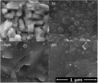
Nanocrystalline diamond films have been deposited by pulsed electron beam ablation from a single target and on different substrates at room temperature and under argon background gas at 0.5 Pa. The films have been deposited from a highly ordered pyrolytic graphite target on four different substrate materials, which include silicon, stainless steel, sapphire, and cubic boron nitride. Based on experimental measurement data, obtained from various analytical techniques, it has been observed that sp3 bonded carbon content, grain size, film roughness, and nanocrystalline fraction of the films do not seem to be much affected by the type of substrate material used. The thickness of the films, in the range of ∼70–90 nm, seems to be relatively the same irrespective of the substrate material. Hardness measurements have shown that film hardness, ranging between 18.5 and 19.5 GPa, is not remarkably influenced by the type of substrate material.

Type
Article
Copyright
Copyright © Materials Research Society 2015 

Access options

Get access to the full version of this content by using one of the access options below. (Log in options will check for institutional or personal access. Content may require purchase if you do not have access.)

References

REFERENCES

Gruen, D.M.: Ultrananocrystalline diamond in the laboratory and the cosmos. MRS Bull. 10, 771 (2001).Google Scholar
Härtl, A., Schmich, E., Garrido, J.A., Hernando, J., Catharino, S., Walter, S., Feulner, P., Kromka, A., Steinmüller, D., and Stutzmann, M.: Protein-modified nanocrystalline diamond thin films for biosensor applications. J. Nat. Mater. 3, 736 (2004).Google Scholar
Zhang, J., Su, D.S., Blume, R., Schlögl, R., Wang, R., Yang, X., and Gajovic, A.: Surface chemistry and catalytic reactivity of nanodiamond for the steam-free dehydrogenation of ethylbenzene. J. Angew. Chem. 49, 8640 (2010).Google Scholar
Michaelson, Sh., Ternyak, O., Akhvlediani, R., Hoffman, A., Lafosse, A., Azria, R., Williams, O.A., and Gruen, D.M.: Hydrogen concentration and bonding configuration in polycrystalline diamond films: From micro- to nano-metric grain size. J. Appl. Phys. 102, 113516 (2007).Google Scholar
Mortet, V., Zhang, L., Eckert, M., D’Haen, J., Soltani, A., Moreau, M., Troadec, D., Neyts, E., De Jaeger, J.C., Verbeeck, J., Bogaerts, A., Van Tendeloo, G., Haenen, K., and Wagner, P.: Grain size tuning of nanocrystalline chemical vapor deposited diamond by continuous electrical bias growth: Experimental and theoretical study. Phys. Status Solidi A 209, 1675 (2012).Google Scholar
Klauser, F., Steinmuller-Nethl, D., Kaindl, R., Bertel, E., and Memmel, N.: Raman studies of nano- and ultra-nanocrystalline diamond films grown by hot-filament CVD. Chem. Vap. Deposition 16, 127 (2010).Google Scholar
Gruen, D.M.: Nanocrystalline diamond films. Annu. Rev. Mater. Sci. 29, 211 (1999).Google Scholar
Davies, R.D.: Diamond (Adam Hilger, Bristol, UK, 1984).Google Scholar
Spear, K.E. and Dismukes, J.P.: Synthetic Diamond: Emerging CVD Science and Technology (John Wiley & Sons Inc., New York, 1993).Google Scholar
Donato, M.G., Faggio, G., Messina, G., Santangelo, S., Marinelli, M., Milani, E., Pucella, G., and Verona-Rinati, G.: Raman and photoluminescence analysis of CVD diamond films: Influence of Si-related luminescence centre on the film detection properties. Diamond Relat. Mater. 13, 923 (2004).Google Scholar
Birrell, J., Gerbi, J.E., Aiciello, O., Gibson, J.M., Johnson, J., and Carlisle, J.A.: Interpretation of the Raman spectra of ultrananocrystalline diamond. Diamond Relat. Mater. 14, 86 (2005).Google Scholar
Vlasov, I.I., Ralchenko, V.G., Goovaerts, E., Saveliev, A.V., and Kanzyuba, M.V.: Bulk and surface-enhanced Raman spectroscopy of nitrogen-doped ultrananocrystalline diamond films. Phys. Status Solidi A 203, 3028 (2006).Google Scholar
Popov, C., Bliznakov, S., and Kulisch, W.: Influence of the substrate nature on the properties of nanocrystalline diamond films. Diamond Relat. Mater. 16, 740 (2007).Google Scholar
Ballutaud, D., Jomard, F., Theys, B., Kociniewski, T., Rzepka, E., Girard, H., and Saada, S.: Sp3/sp2 character of the carbon and hydrogen configuration in micro- and nanocrystalline diamond. Diamond Relat. Mater. 17, 451 (2008).Google Scholar
Hongyan, P., Jiajing, S., and Guilong, Y.: Study of nanocrystalline diamond film deposited rapidly by 500 W excimer laser. Chin. J. Laser 9, 201 (2000).Google Scholar
Ou, Y., Guo, J., and Yan, X.: Growth of nanocrystalline diamond films by pulsed laser deposition in oxygen atmosphere. Nat. Sci. J. Xiangtan Univ. 25, 30 (2003).Google Scholar
Pukha, V.E., Stetsenko, A.N., Dub, S.N., and Lee, J.K.: Nanocrystalline diamond thin films deposited from C60 monoenergetic fullerene ion beam. J. Nanosci. Nanotechnol. 7, 1370 (2007).Google Scholar
Mounier, E., Bertin, F., Adamik, M., Pauleau, Y., and Barna, P.B.: Effect of the substrate temperature on the physical characteristics of amorphous carbon films deposited by d.c. magnetron sputtering. Diamond Relat. Mater. 5, 1509 (1996).Google Scholar
Henda, R. and Alshekhli, O.: Pulsed electron beam deposition of nanocrystalline diamond. MRS Online Proc. Libr. 1505, 6 (2013).Google Scholar
Alshekhli, O. and Henda, R.: Hydrogen-free deposition of nanocrystalline diamond by channel-spark electron beam ablation. ECS J. Solid State Sci. Technol. 3, M21 (2014).Google Scholar
Harshavardhan, K.S. and Strikovski, M.: Pulsed electron-beam deposition of high temperature superconducting films for coated conductor applications. In Second-Generation HTS Conductors, Goyal, A. ed.; Springer: New York, 2005; pp. 109133.Google Scholar
Strikovski, M. and Harshavardhan, K.S.: Parameters that control pulsed electron beam ablation of materials and film deposition processes. Appl. Phys. Lett. 82, 853 (2003).Google Scholar
Alshekhli, O.: PhD Thesis Dissertation, Laurentian University, Canada, 2013.Google Scholar
Ferrari, A.C. and Robertson, J.: Raman spectroscopy of amorphous, nanostructured, diamond-like carbon, and nanodiamond. Philos. Trans. R. Soc. Lond. Ser. A 362, 2477 (2004).Google Scholar
Prawer, S., Nugent, K.W., Jamieson, D.N., Orwa, J.O., Bursill, L.A., and Peng, J.L.: The Raman spectrum of nanocrystalline diamond. J. Chem. Phys. Lett. 332, 93 (2000).Google Scholar
Osswald, S., Mochalin, V.N., Havel, M., Yushin, G., and Gogotsi, Y.: Phonon confinement effects in the Raman spectrum of nanodiamond. Phys. Rev. B 80, 75419 (2009).Google Scholar
Filik, J., Harvey, J.N., Allan, N.L., and May, P.W.: Raman spectroscopy of nanocrystalline diamond: An ab initio approach. Phys. Rev. B 74, 035423 (2006).Google Scholar
Bhattacharya, A.K. and Nix, W.D.: Analysis of elastic and plastic deformation associated with indentation testing of thin films on substrates. Int. J. Solids Struct. 24, 1287 (1988).Google Scholar
Yang, W., Lu, F., and Cao, Z.: Growth of nanocrystalline diamond protective coatings on quartz glass. J. Appl. Phys. 91, 10068 (2002).Google Scholar
Narayan, R., Wei, W., Jin, C., Andara, M., Agarwal, A., Gerhardt, R., Shih, C., Lin, S., Su, Y., Ramamurti, R., and Singh, R.: Microstructural and biological properties of nanocrystalline diamond coatings. J. Diamond Relat. Mater. 15, 1935 (2006).Google Scholar
Wiora, M., Sadrifar, N., Brühne, K., Gluche, P., and Fecht, H.: Correlation of microstructure and tribological properties of dry sliding nanocrystalline diamond coatings. In Proceedings of 3rd European Conference on Tribology, Vol. 1, Franek, F. ed.; Vienna, Austria, 2011; pp. 293298.Google Scholar
Henda, R. and Alshekhli, O.: Estimation of requirements for the formation of nanocrystalline diamond driven by electron beam ablation. IEEE Trans. Plasma Sci. 43, 461 (2015).Google Scholar