


Introduction
Power electronics is the branch of electronics specifically dealing with collecting, delivering, and storing energy, including general and local/commodity energy supplies, by conversion and control of electrical power.Reference Hart1 Specific applications range from power supply systems to motor vehicle drives,Reference Hamada, Nagao, Ajioka and Kawai2 photovoltaic and fuel cell converters, inverters, and high-frequency heating,Reference Samago, Lucia, Mediano and Burdio3 among many others. The impact of power electronics has already been significant and is anticipated to be even more so in the future for efficient energy production and management.
As in most other electronics areas, silicon also has been the predominant semiconductor in power electronics to date. However, with wide bandgap materials power electronic components are faster, smaller, more efficient, and more reliable than their Si-based counterparts. Moreover, they permit the operation of devices at higher voltages, temperatures, and frequencies,Reference McNutt, Passmore, Fraley, McPherson, Shaw, Olejniczak and Lostetter4 making it possible to reduce volume and weight in a wide range of applications. This could lead to large energy savings in industrial and consumer appliances, accelerate widespread use of electric vehicles and fuel cells, and integrate renewable energy into the electric grid.
The power electronics market as a whole was about $20 billion in 2012, and power electronics will remain one of the most attractive branches of the semiconductor industry over the next decade.5 The latest power electronics market forecasts6 predict an increase of 60% for low-voltage technologies (below 900 V) by the year 2020, accompanied by an approximately 100% market increase for medium (1.2–1.7 kV) and high voltage (2 kV and above) technologies. This implies that the largest market increase in this sector over the next decade (medium and high voltage) will rely on semiconductor technologies beyond silicon (also see article by Okumura in this issue). This can be likened to a second revolution, equivalent to the introduction of large scale fabrication of silicon complementary metal oxide semiconductor (CMOS) technology, which led to the commoditization of electronics and formed the basis of our modern technological era. The power electronics revolution could be setting the basis for a world centered on greener technologies: improved energy conversion efficiencies, faster switching, and more compact, lighter systems with better thermal management and tolerance will have tremendous impact on industrialization and energy systems, encompassing energy savings, renewable energy systems, and electric/hybrid vehicles, to name a few. This would enable compelling cost and energy savings and help cope with the progressive exhaustion of fossil fuels and reduce anthropogenic greenhouse gas emissions in the atmosphereReference Bose7 (Figure 1). New electronic materials (i.e., wide bandgap semiconductors such as SiC and GaN) are at the very center of this 21st century revolution.

Figure 1. World’s anthropogenic greenhouse gas emissions from 1970 to 2004, expressed in gigatons CO2 equivalent.Reference Mueller, Sanchez, Hansen, Drachev, Chung, Thomas, Zhang, Loboda, Dudley, Wany, Wu, Byrappa, Raghotamachar and Choi20
Such a transformation does not happen easily. A whole new set of technologies needs to be developed, including novel substrate materials, epitaxial film growth and doping, and device and circuit engineering, as well as appropriate thermal interfaces, interconnects, and packaging. These need to be brought from the laboratory up to full integration on a pilot production line and evaluated in terms of yield, quality, and reliability before being ramped up to large-scale production. Anyone familiar with the evolution in complexity of CMOS processes, especially over the last two decades, can easily picture the pace at which research and development must happen in order for this scale up to occur.
The current drive toward power electronics technology is also exemplified by the recent announcement by Governor A.M. Cuomo of the state of New York, USA, publicly announcing “100 Businesses Led by GE to Join $500 Million Partnership with State to Develop Next-Generation Power Electronics, Creating Thousands of Jobs in Capital Region and Upstate.”8 The further development of fast and efficient transportation such as the bullet trains in Japan and China, the expanding market of fully electric cars as pursued by Tesla Motors, Inc., and the progress in exploiting and storing energy from renewable sources, will all undoubtedly lead to a radical and greener transformation of our modern world where power electronics is central. This issue of MRS Bulletin offers a snapshot of the worldwide efforts and knowledge developed in these areas from a materials perspective, allowing us to envisage a power electronics revolution.
The impact of power electronics has already been significant and is anticipated to be even more so in the future for efficient energy production and management. B.K. Bose explains how power electronics will help enhance energy efficiency in areas such as harvesting renewable energies, energy storage, electric vehicles as well as energy savings by implementing a “smart grid.”Reference Bose7 The smart grid is enabled by a combination of power electronics, automation control, and, possibly, artificial intelligence. Elevated CO2 emissions from the combustion of fossil fuels as illustrated in Figure 1, have been recognized as a major source of accelerated global warming, which in the long run may result in unsustainable costs to our society in terms of health and quality of life.9 As stated in the most recent Intergovernmental Panel on Climate Change: “Innovation and investments in environmentally sound infrastructure and technologies can reduce greenhouse gas emissions and enhance resilience to climate change (very high confidence).”10 Significant reductions in cost and CO2 emissions are expected to result in the long run from the widespread use of power electronics and related automation control technologies anticipated over the coming decades.
Specific devices with efficiencies approaching 98–99%,Reference Bose7 ultra-fast switching capabilities, and high resiliency to high temperature and other harsh environmental conditions are required for power electronics, which was officially born with the silicon power metal oxide semiconductor field-effect transistor (MOSFET) entering the market in the late 1970s.Reference Bose7 While the early days of power electronics relied on silicon, ever increasing requirements for higher efficiencies and resiliency to harsh environments (such as voltages up to 3 kV and temperatures in excess of 400°C) have led the research community to consider semiconductor materials beyond silicon. In particular, two wide bandgap materials, SiC and GaN, have emerged as suitable near-term candidates. Both SiC and GaN can sustain a substantially higher critical electric field than Si, and ON-resistance behavior that can be achieved as a function of operating voltage is substantially more favorable for SiC, and ultimately GaN devices, which would result in up to a tenfold loss reduction compared to silicon devicesReference Lu11 (see the article by Dimitrijev et al. in this issue).
However, from a practical point of view, the full advantages of SiC and GaN devices are limited by the crystalline quality of their respective thin-film materials (see for example the articles by M. Kitabatake and Hilt et al. in this issue). The articles in this MRS Bulletin issue specifically address this central challenge to the materials research community.
Applications and figures of merit
Wide bandgap materials allow power electronic components to be faster, smaller, more efficient, and more reliable than their Si-based counterparts. Moreover, they permit the operation of devices at higher voltages, temperatures, and frequencies,Reference Okumura12 making it possible to reduce volume and weight in a wide range of applications. This could lead to large energy savings in industrial and consumer appliances, accelerate widespread use of electric vehicles and fuel cells, and help integrate renewable energy into the electric grid.
When using wide bandgap materials, several energy-related benefits will result in a greener environment by eliminating up to 90% of power losses currently occurring during electric conversion.Reference Abuishmais and Undeland13 Wide bandgap devices can operate at a voltage 10 times higher than Si-based power devices, because of their higher maximum electric field and operating temperatures of well over 300°C, twice the maximum operating temperature of Si-based devices. Theoretically, the operating frequency is at least 10 times higher, thereby opening up a range of new applications, such as compact radio frequency amplifiers. In practice, the latter property is difficult to realize for SiC, so GaN is used to fabricate high-performance, high-frequency devices.
Once wide bandgap materials and power devices have matured, substrate material and manufacturing costs are expected to decrease, and the devices will be widely used in highly efficient variable speed drives in motors or as compact power supplies in consumer electronics. They can convert direct current (DC) electricity generated from wind and solar energy into alternating current electricity used at home and in businesses with reduced energy losses. In addition, the transformer size could be reduced by a factor of 10 or more. These devices will also find applications in efficient high-voltage DC power transmission lines, while for automotive applications the use of wide bandgap materials will considerably reduce electricity loss during vehicle battery recharging. The greater efficiency possible in operating electric traction drives and the ability to tolerate high operating temperatures can also considerably reduce the size of automotive cooling systems.
There are several questions and ongoing discussions about GaN versus SiC, the possible devices, and which material is best suited for various applications. For power switching applications, the material properties of both SiC and GaN are superior to those of Si. An overview of the material properties of SiC and GaN compared to gallium arsenide, the most commonly used III–V low bandgap material, and Si is given in Table I.Reference Tolbert, Ozpineci, Islam and Chinthavali14
Table I. Overview of the material properties of Si, GaAs, GaN, and 4H-SiC.Reference Tolbert, Ozpineci, Islam and Chinthavali14

* Values of corresponding heterostructures.
The high electric breakdown field of both SiC and GaN compared to that of Si allows these devices to operate at higher voltages and with lower on-resistance while higher electron mobility and electron saturation velocity allow for higher operating frequency. The electron mobility of GaN is higher than that of SiC indicating that GaN is the best material for very high-frequency applications, but SiC has the highest thermal conductivity indicating that SiC devices can operate at higher power densities. The relatively poor heat conductivity of GaN makes the heat management of GaN power devices a challenge.
The availability of high-quality material has resulted in varying paces of development in GaN and SiC. SiC is ahead in development and commercialization due to readily available six-inch (150 mm) substrates, where GaN bulk substrates are only available at two inches (50 mm) and below. This slower pace of GaN development has been further exacerbated by the need for heteroepitaxy: GaN devices are most commonly grown on non-native SiC or Si substrates, requiring a buffer layer to accommodate the difference in lattice parameters and equally important, the difference in thermal expansion coefficient (see the article by Semond in this issue). In contrast, SiC devices are fabricated via homoepitaxy, analogous to Si, in that the SiC epitaxial layer is formed on a SiC substrate, resulting in an excellent crystallographic match between the two. The SiC throughout also provides excellent thermal and good electrical conductivity from top to bottom of the wafer. Homoepitaxial SiC devices have the advantage that both lateral and vertical devices can be fabricated. SiC lateral MOSFETs are popular high frequency devices, while vertical SiC devices include Schottky diodes, PIN diodes (consisting of p-type, intrinsic, and n-type materials), junction field-effect transistors (JFETs), bipolar junction transistors, and normally OFF MOSFET devices.Reference Agarwal, Das, Krishnaswami, Palmour, Richmond, Ryu, Dudley, Gouma, Kimoto, Neudeck and Saddow15–Reference Kimoto, Suda, Yonezawa, Asano, Fukuda and Okumura18 As an example, a cross-section of a vertical double MOSFET (DMOSFET) SiC power device is shown in Figure 2a. The drawback of most typical SiC JFETs is that they are normally ON structures, which designers are reluctant to use, because the device conducts current when a gate bias is not applied. For SiC MOSFETs, which are normally OFF devices, the primary challenge is the scaling up of the device size to conduct high current while maintaining high device yield and good reliability (see the article by Zetterling in this issue).
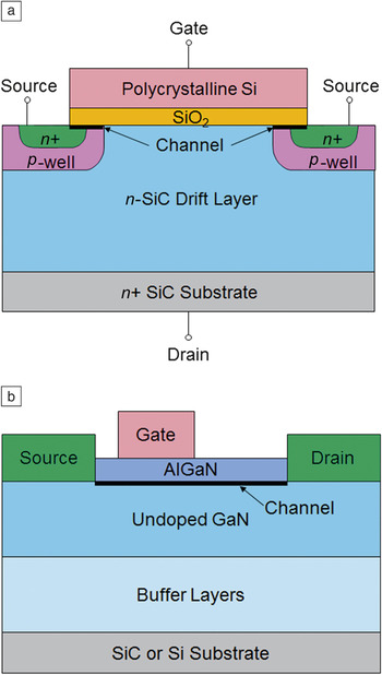
Figure 2. Cross-sections of typical wide bandgap power devices: (a) Vertical double metal oxide semiconductor SiC metal oxide semiconductor field-effect transistor, and (b) lateral GaN high-electron-mobility transistors.
Heteroepitaxial GaN devices are still mostly restricted to lateral devices due to the required buffer layer on the nonnative substrate, although the technology for GaN substrates is progressing, as Davis indicates in his article in this issue. The disadvantage is that lateral devices generally require more space, which impacts yield. Lateral devices are also limited in their operating voltage because the large electric field must be sustained both across the surface of the device and in the buffer layer, especially when a narrow bandgap material such as Si is used as the substrate material. Both lateral GaN Schottky diodes and high-electron-mobility transistors (HEMTs) have been fabricated (Figure 2b).
Radio frequency (RF) GaN-on-SiC HEMTs are being fabricated today for use at high frequencies. Their primary application is for defense systems where cost is not the primary factor. RF GaN-on-Si devices are also being developed to primarily target applications such as wireless communication. Another application for the GaN-on-Si product is lower switching voltage (600 V and lower) power electronics.Reference Jatal, Baumann, Tonisch, Schwierz and Pezoldt19 However, improving the starting material quality and yield, increasing the wafer diameter, reducing wafer cost, and developing normally OFF devices are needed in order to compete with the current state-of-the-art Si devices.
In summary, it is generally believed that lateral heteroepitaxial GaN-on-Si power devices will displace devices below 600 V in the power switching market, while homoepitaxial vertical SiC devices will dominate in power switching applications above 600 V. This is mainly because homoepitaxial SiC will remain lower in cost compared to heteroepitaxial GaN-on-Si, because the device processing on homoepitaxial SiC is simpler. At the same time, compared to the much more difficult GaN-on-Si epitaxy, the SiC homoepitaxy results in higher quality substrates with lower defect density. Furthermore, because GaN-on-Si does not have the high thermal conductivity that homoepitaxial SiC has, homoepitaxial SiC may be favored for high-temperature applications.
The materials challenge
In addition to the increase in wafer diameter up to 150 mm, SiC bulk substrates have seen fast improvement in quality in recent years, with reductions in micropipe (hollow defects that extend through the film) density, dislocation density, and surface defects,Reference Mueller, Sanchez, Hansen, Drachev, Chung, Thomas, Zhang, Loboda, Dudley, Wany, Wu, Byrappa, Raghotamachar and Choi20 which had previously limited the performance of SiC devices. These advances have addressed many challenges associated with SiC devices and have increased performance and yield, allowing high voltage devices to be brought to market.Reference Mueller, Sanchez, Hansen, Drachev, Chung, Thomas, Zhang, Loboda, Dudley, Wany, Wu, Byrappa, Raghotamachar and Choi20 The development of heteroepitaxial SiC on silicon is still in relatively early stages, and although there are large gains in terms of cost and wafer diameter that can be achieved with this technology, more work is needed to be able to fabricate high performance devices. The biggest challenge for SiC therefore is the continued improvement in the quality of layers and substrates, while reducing the unit cost, to allow further market penetration.
Bulk GaN would also be an attractive substrate for devices, as shown by devices developed as early as 2007 by Toyota;Reference Sugimoto, Ueda, Kanechika and Soejima21 however, as mentioned above, GaN substrate wafers are currently only available with diameters up to two inches. This challenge has been taken up in different ways, with continued development of very high quality small wafers using high pressure and temperature by Amano and othersReference Amano22 alongside various hydride vapor epitaxy-based techniques. In addition, Soitec has applied their Smart Cut technique, a wafer-bonding and layer-splitting processes allowing transfer of thin layers of crystalline material from a donor substrate to another substrate. This has allowed the fabrication of high-quality 150 mm GaN layers bonded to ceramic substrates.23
In the absence of viable low cost GaN bulk substrates, development for power electronics has occurred on a variety of heterosubstrates, with the most popular being SiC, sapphire, and silicon.Reference Pearton24 GaN grown on SiC has excellent thermal, electrical, and physical characteristics for GaN devices, but the small size of the substrates and high cost have meant that this model is poorly suited for the power transistor market. Sapphire has many interesting properties, such as lower cost and availability of large diameter wafers, but its properties as a thermal insulator have meant that although it is effective as a substrate for light-emitting devices (LEDs), it is difficult to use for fabricating high performance devices. This has left silicon as a highly promising substrate for GaN-based power devices. It should be noted that the silicon is oriented (111) rather than the standard (100) in order to have trigonal symmetry, which better matches the hexagonal symmetry of GaN. With silicon substrates easily available in 150 mm and 200 mm diameters and GaN on 200 mm silicon substrate growth capabilities as early as 2009,Reference Boyd, Degroote, Leys, Schulte, Rockenfeller, Luenenbuerger, Germain, Kaeppeler and Heuken25 this approach allows integration using standard electronics processing lines. This has the potential to reduce costs for industrialization of GaN based power devices as a product and allows large-scale, high-quality production to be achieved more easily (see the article by Semond in this issue).
GaN growth on silicon must treat two important issues for the power transistor market: the breakdown voltage (or leakage current) and the phenomenon of current collapse. Current collapse is the effect whereby after stressing a device at high reverse bias, the resistance of the device in forward bias is significantly increased,Reference Vetury, Zhang, Keller and Mishra26 which is attributed to either surface statesReference Vetury, Zhang, Keller and Mishra26 or defects and impurities in the grown material.Reference Selvaraj, Selvaraj and Egawa27 For GaN on silicon growth, the silicon does not add significantly to the breakdown voltage of devices, and as the substrate will typically be grounded in industrial applications, it must be insulated from the drain of the transistor using GaN (and AlN or AlGaN) layers, even in lateral devices. It is also important that the leakage current between the drain and the substrate be very low, in order to improve the device performance. As a result, despite a theoretical breakdown voltage of around 3 MV/cm, a thickness of 4 to 5 µm is necessary for a transistor to operate at 600 V.28 As GaN has a significantly larger thermal expansion coefficient than silicon, the strain induced by cooling the wafers from the growth temperature can be challenging to control when growing thicker films. But, controlling the strain is necessary to ensure that the wafers are sufficiently flat and crack free after growth, which allows processing into transistors at a later date.
One way to overcome the requirement for thick films is to remove the silicon under the transistor. This removes the contact with the ground and also avoids lateral leakage passing through the substrate.Reference Srivastava, Das, Visalli, Derluyn, Van Hove, Malinowski, Marcon, Geens, Cheng, Degroote, Leys, Germain, Decoutere, Mertens and Borghs29 An alternative way to isolate the transistor from the ground is to use silicon-on-insulator wafers as substrates.Reference Jiang, Liu, Lu and Chen30 Since both of these techniques add cost to the overall device, a commonly used alternative is using doping to form deep traps, such as using carbonReference Kato, Satoh, Sasaki, Masayuki and Yoshida31 or ironReference Aggerstam, Sjödin and Lourdudoss32 as dopants. Carbon doping has been shown to greatly increase the breakdown voltageReference Kato, Satoh, Sasaki, Masayuki and Yoshida31 and is the preferred choice, as iron has a strong memory effect, which can strongly impact the resistance of the channel that is grown after the bulk layer.Reference Aggerstam, Sjödin and Lourdudoss32 Carbon also has the advantage of being an intrinsic dopant and therefore can be controlled using the epitaxial growth conditions in metal-organic vapor-phase epitaxy.Reference Stringfellow33 However, this use of traps to make the material more insulating must be carefully controlled, as carbon has been identified as a potential source of current collapse.Reference Selvaraj, Selvaraj and Egawa27
A commonly discussed aspect in the development of GaN heteroepitaxy is the impact of the high density of dislocations, typically around 1 × 109 cm–2. There is currently little firm evidence that dislocations are a first-order problem for devices, unlike the detrimental effect of edge dislocations on GaN LEDs.Reference Dai, Schubert, Kim, Kim, Schubert, Koleske, Crawford, Lee, Fischer, Thaler and Banas34 It is likely that a higher dislocation density will affect the reliability and lifetime of devices, so efforts will be made to continue improving the crystalline quality of the material.
For both GaN and SiC, there are challenges in device packaging. Both materials are capable of operating at higher temperatures and frequencies than equivalent silicon devices. Although it is difficult to compete directly on a cost per transistor basis with silicon, if the packaging is optimized for higher frequency operation, the resulting smaller passive componentsReference Friedli, Round, Hassler and Kolar35 can reduce cost at the system level. Equally, higher operating temperatures are possible with SiC and GaN than with silicon, reducing the size and cost of the required cooling. As a consequence, appropriate driver or control electronics, need to be developed to allow such high-frequency and high-temperature operation to ensure that the final products take full advantage of the performance of SiC or GaN devices.
Summary and perspectives
Wide bandgap semiconductors such as GaN and SiC are next generation materials for power electronics, showing strong potential and promising significant advantages over Si-based conventional electronics. Both materials are superior to Si from different points of view, and a revolution toward greener and more efficient technologies and devices is anticipated. However, there are also significant challenges to consider, including the materials science and technology details and device fabrication. Depending on the proposed solutions, cost reduction plays an important role for effective industrial implementation, production, and market penetration. Market forecasts predict a strong increase in the next 5–10 years for power electronics technologies and an important contribution is expected to come from the use of wide bandgap semiconductors.
It is worth noting that the development of semiconductors, in particular of wide bandgap semiconductors, and progress of their technologies, tends to trigger the development of other materials and new devices and technologies. Initial integration with Si, but in future integration with other materials as well, such as oxides, organics, chalcogenides, and graphene, promises new directions for applied science and technology. New integrated composite architectures, interfaces, and the utilization of shape and nanoscale synergetic effects by using wide bandgap semiconductors could further enhance the electronics revolution, possibly through new physical phenomena. Note that advances in this space will have to be treated holistically, as improved interconnects and packaging will need to be developed in parallel to cope, for example, with harsh operating environments (see the article by Zetterling in this issue).
Better efficiency but also new functionality or multiple functionalities for novel applications, are envisioned as well. For example, SiC is a lightweight material and has good wear, thermal stability, and mechanical properties, and, at the same time, it shows outstanding electrical and thermal properties. SiC is an old material, but it continues to be novel. Historically, development and research in SiC shows a strongly multidimensional pattern. For SiC, the development was dictated by the needs imposed by changes in society. SiC can be considered to be a mirror of society’s needs at different moments of recent history. The same can be said for GaN as well, as it has already shown crucial applications beyond electronics into opto-electronics and microelectromechanical systems. GaN and SiC are key materials for the electronics revolution and have a direct, powerful impact on other fields such as GaN for optoelectronic devices (note the 2014 Nobel Prize awarded for blue LEDs36).
Further progress requires fundamental research on properties and synthesis, or processing. For synthesis or processing for devices, the challenge is to decrease the required synthesis or processing temperature of SiC to values similar to those for conventional Si technologies. Some progress in this direction has already been demonstrated.Reference Kusumori, Muto and Brito37,38 This can be very important because high quality heteroepitaxial growth of 4H-SiC films at low temperatures and on substrates with different orientations could be easily produced.
The articles in this issue of MRS Bulletin indicate that some approaches, technologies, and developments are mature enough for implementation and commercialization, while others are still in the early stages and will require sustained research efforts. Beyond SiC and GaN, new classes of materials as diverse as ZnO, Ga2O3, and diamond, currently still very far from technological implementation, may prove to be an even more efficient newer generation of wide bandgap materials for power electronics in the coming decades.
This issue presents the state of the art in the field of power electronics using wide bandgap semiconductors. This is also an invitation to promote scientific collaboration, exchange ideas, and debate on different solutions to problems in the development of wide bandgap semiconductors for power electronics. It is hoped that this issue will be a source of inspiration and motivation for younger generations of researchers.
Acknowledgments
Kurt Gaskill (NRL), Tomas Palacios and Bin Lu (MIT), and Petre Badica (NIMP, Romania) are acknowledged for advice and helpful discussions. FI acknowledges the Australian Research Council support through the grant FT120100445 (Future Fellowship).


