Hostname: page-component-8448b6f56d-mp689 Total loading time: 0 Render date: 2024-04-23T11:47:20.270Z Has data issue: false hasContentIssue false

Damage accumulation in diamond during ion implantation

Published online by Cambridge University Press:  12 February 2015

Roman A. Khmelnitsky*
Affiliation:
Tal Division of Solid State Physics, Lebedev Physical Institute of RAS, Moscow 119991, Russia
Valeriy A. Dravin
Affiliation:
Tal Division of Solid State Physics, Lebedev Physical Institute of RAS, Moscow 119991, Russia
Alexey A. Tal
Affiliation:
Tal Division of Solid State Physics, Lebedev Physical Institute of RAS, Moscow 119991, Russia
Evgeniy V. Zavedeev
Affiliation:
Natural Sciences Center, Prokhorov General Physics Institute of RAS, Moscow 119991, Russia; and National Research Nuclear University MEPhI, Moscow 115409, Russia
Andrey A. Khomich
Affiliation:
Natural Sciences Center, Prokhorov General Physics Institute of RAS, Moscow 119991, Russia; and Kotelnikov Institute of Radioengineering and Electronics of RAS, Moscow Region, Fryazino 141120, Russia
Alexander V. Khomich
Affiliation:
Kotelnikov Institute of Radioengineering and Electronics of RAS, Moscow Region, Fryazino 141120, Russia
Alexander A. Alekseev
Affiliation:
Technological Institute for Superhard and Novel Carbon Materials, Moscow Region, Troitsk 142190, Russia
Sergey A. Terentiev
Affiliation:
Technological Institute for Superhard and Novel Carbon Materials, Moscow Region, Troitsk 142190, Russia
*
a)Address all correspondence to this author. e-mail: roma@lebedev.ru
Get access

Abstract

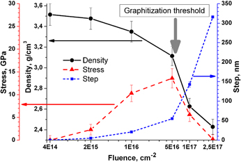
Single-crystalline diamond plates were implanted by He+ ions with a set of energies and fluences that ensure uniform radiation damage (RD) in a 670-nm-thick layer. Implantation is carried out at a wide range of fluences, which allows one to cover the range of RD levels from very low to complete graphitization of diamond. Using the measurement data on the bending of diamond plates and the surface swelling of the ion-implanted material, we calculate the mechanical stress and the density of diamond for various levels of RD. Diamonds with various levels of RD are investigated by the Raman scattering and optical transmission methods. We establish that, above the graphitization threshold, the diamond phase almost completely disappears as the RD level increases, while the fraction of sp2 material sharply increases. Such a material is unexpectedly ductile. It cannot be restored to diamond even by annealing under a pressure corresponding to thermodynamic stability of diamond.

Type
Articles
Copyright
Copyright © Materials Research Society 2015 

Access options

Get access to the full version of this content by using one of the access options below. (Log in options will check for institutional or personal access. Content may require purchase if you do not have access.)

Footnotes

Contributing Editor: William J. Weber

References

REFERENCES

Campbell, B., Choudhury, W., Mainwood, A., Newton, M., and Davies, G.: Lattice damage caused by the irradiation of diamond. Nucl. Instrum. Methods Phys. Res., Sect. A 476, 680 (2002).CrossRefGoogle Scholar
Berdermann, E.: Advanced diamond particle detectors. Nucl. Phys. News 19(2), 25 (2009).Google Scholar
Jelezko, F. and Wrachtrup, J.: Single defect centres in diamond: A review. Phys. Status Solidi A 203(13), 3207 (2006).CrossRefGoogle Scholar
Orwa, J.O., Greentree, A.D., Aharonovich, I., Alves, A.D.C., Van Donkelaar, J., Stacey, A., and Prawer, S.: Fabrication of single optical centres in diamond—A review. J. Lumin. 130, 1646 (2010).Google Scholar
Kalish, R.: Diamond as a unique high-tech electronic material: Difficulties and prospects. J. Phys. D: Appl. Phys. 40, 6467 (2007).Google Scholar
Prins, J.F.: Ion implantation of diamond for electronic applications. Semicond. Sci. Technol. 18, 27 (2003).Google Scholar
Uzan-Saguy, C., Cytermann, C., Brener, R., Richter, V., Shaanan, M., and Kalish, R.: Damage threshold for ion-beam induced graphitization of diamond. Appl. Phys. Lett. 67(9), 1194 (1995).Google Scholar
Yamada, H., Chayahara, A., Umezawa, H., Tsubouchi, N., Mokuno, Y., and Shikata, S.: Fabrication and fundamental characterizations of tiled clones of single-crystal diamond with 1-inch size. Diamond Relat. Mater. 24, 29 (2012).CrossRefGoogle Scholar
Liao, M., Rong, Z., Hishita, S., Imura, M., Koizumi, S., and Koide, Y.: Nanoelectromechanical switch fabricated from single crystal diamond: Experiments and modeling. Diamond Relat. Mater. 24, 69 (2012).CrossRefGoogle Scholar
Olivero, P., Amato, G., Bellotti, F., Budnyk, O., Colombo, E., Jakšić, M., Manfredotti, C., Pastuović, Ž., Picollo, F., Skukan, N., Vannoni, M., and Vittone, E.: Direct fabrication of three-dimensional buried conductive channels in single crystal diamond with ion microbeam induced graphitization. Diamond Relat. Mater. 18, 870 (2009).Google Scholar
Greentree, A.D., Olivero, P., Draganski, M., Trajkov, E., Rabeau, J.R., Reichart, P., Gibson, B.C., Rubanov, S., Huntington, S.T., Jamieson, D.N., and Prawer, S.: Critical components for diamond-based quantum coherent devices. J. Phys.: Condens. Matter 18, 825 (2006).Google Scholar
Zaitsev, A.M. and Dobrinets, I.A.: Carbon nanodots made on diamond surface by focused ion beam. Phys. Status Solidi A 203(5), 35 (2006).Google Scholar
Riedrich-Moller, J., Kipfstuhl, L., Hepp, C., Neu, E., Pauly, C., Mucklich, F., Baur, A., Wandt, M., Wolff, S., Fischer, M., Gsell, S., Schreck, M., and Becher, C.: One- and two-dimensional photonic crystal microcavities in single crystal diamond. Nat. Nanotechnol. 7, 69 (2012).Google Scholar
Hickey, D.P., Jones, K.S., and Elliman, R.G.: Amorphization and graphitization of single-crystal diamond—A transmission electron microscopy study. Diamond Relat. Mater. 18, 1353 (2009).Google Scholar
Fairchild, B.A., Rubanov, S., Lau, D.W.M., Robinson, M., Suarez-Martinez, I., Marks, N., Greentree, A.D., McCulloch, D., and Prawer, S.: Mechanism for the amorphisation of diamond. Adv. Mater. 24(15), 2024 (2012).Google Scholar
Morehead, F.F. and Crowder, B.L.: A model for the formation of amorphous Si by ion bombardment. Radiat. Eff. 6, 27 (1970).Google Scholar
Gibbons, J.F.: Ion implantation in semiconductors—Part II: Damage production and annealing. Proc. IEEE 60, 1062 (1972).Google Scholar
Wendler, E.: Mechanisms of damage formation in semiconductors. Nucl. Instrum. Methods Phys. Res., Sect. B 267, 2680 (2009).Google Scholar
Prins, J.F.: Graphitization and related variable-range-hopping conduction in ion-implanted diamond. J. Phys. D: Appl. Phys. 34, 2089 (2001).Google Scholar
Newton, M.E., Campbell, B.A., Twitchen, D.J., Baker, J.M., and Anthony, T.R.: Recombination-enhanced diffusion of self-interstitial atoms and vacancy-interstitial recombination in diamond. Diamond Relat. Mater. 11, 618 (2002).Google Scholar
Orwa, J.O., Santori, C., Fu, K.M.C., Gibson, B., Simpson, D., Aharonovich, I., Stacey, A., Cimmino, A., Balog, P., Markham, M., Twitchen, D., Greentree, A.D., Beausoleil, R.G., and Prawer, S.: Engineering of nitrogen-vacancy color centers in high purity diamond by ion implantation and annealing. J. Appl. Phys. 109, 083530 (2011).Google Scholar
Watkins, G.D.: What we have learned about intrinsic defects in silicon: A help in understanding diamond? Phys. Status Solidi A 186(2), 167 (2001).Google Scholar
Pelaz, L., Marqués, L.A., and Barbolla, J.: Ion-beam-induced amorphization and recrystallization in silicon. J. Appl. Phys. 96(11), 5947 (2004).Google Scholar
Crookes, W.: On the action of radium emanations on diamond. Proc. R. Soc. London LXXIV, 47 (1904).Google Scholar
Amekura, H. and Kishimoto, N.: Effects of high-fluence ion implantation on colorless diamond selfstanding films. J. Appl. Phys. 104, 063509 (2008).Google Scholar
Lagomarsino, S., Olivero, P., Calusi, S., Gatto Monticone, D., Giuntini, L., Massi, M., Sciortino, S., Sytchkova, A., Sordini, A., and Vannoni, M.: Complex refractive index variation in proton-damaged diamond. Opt. Express 20(17), 19382 (2012).Google Scholar
Collins, A.T.: Optical centres produced in diamond by radiation damage. New Diamond Front. Carbon Technol. 17(2), 47 (2007).Google Scholar
Prawer, S. and Kalish, R.: Ion-beam-induced transformation of diamond. Phys. Rev. B 51(22), 15711 (1995).Google Scholar
Kalish, R., Reznik, A., Nugent, K.W., and Prawer, S.: The nature of damage in ion-implanted and annealed diamond. Nucl. Instrum. Methods Phys. Res., Sect. B 148(1–4), 626 (1999).Google Scholar
Steeds, J.W., Charles, S., Davis, T.J., Gilmore, A., Hayes, J., Pickard, D., and Butler, J.E.: Creation and mobility of self-interstitials in diamond by use of a transmission electron microscope and their subsequent study by photoluminescence microscopy. Diamond Relat. Mater. 8, 94 (1999).CrossRefGoogle Scholar
Collins, A.T.: The characterisation of point defects in diamond by luminescence spectroscopy. Diamond Relat. Mater. 1(1), 457 (1992).Google Scholar
Twitchen, D.J., Hunt, D.C., Newton, M.E., Baker, J.M., Anthony, T.R., and Banholzer, W.F.: Electron paramagnetic resonance (EPR) and optical absorption studies of defects created in diamond by electron irradiation damage at 100 and 350 K. Phys. B 273274, 628 (1999).Google Scholar
Orwa, J.O., Nugent, K.W., Jamieson, D.N., and Prawer, S.: Raman investigation of damage caused by deep ion implantation in diamond. Phys. Rev. B 62(9), 5461 (2000).Google Scholar
Prins, J.F., Derry, T.E., and Sellschop, J.P.F.: Volume expansion of diamond during ion implantation. Phys. Rev. B 34(12), 8870 (1984).Google Scholar
Bosia, F., Calusi, S., Giuntini, L., Lagomarsino, S., Giudice, A.Lo., Massi, M., Olivero, P., Picollo, F., Sciortino, S., Sordini, A., Vannoni, M., and Vittone, E.: Finite element analysis of ion-implanted diamond surface swelling. Nucl. Instrum. Methods Phys. Res., Sect. B 268, 2991 (2010).Google Scholar
Bosia, F., Argiolas, N., Bazzan, M., Olivero, P., Picollo, F., Sordini, A., Vannoni, M., and Vittone, E.: Modification of the structure of diamond with MeV ion implantation. Diamond Relat. Mater. 20, 774 (2011).Google Scholar
Bosia, F., Argiolas, N., Bazzan, M., Fairchild, B.A., Greentree, A.D., Lau, D.W.M., Olivero, P., Picollo, F., Rubanov, S., and Prawer, S.: Direct measurement and modelling of internal strains in ion-implanted diamond. J. Phys.: Condens. Matter 25, 385403 (2013).Google Scholar
Khmelnitsky, R.A., Dravin, V.A., Tal, A.A., Latushko, M.I., Khomich, A.A., Khomich, A.V., Trushin, A.S., Alekseev, A.A., and Terentiev, S.A.: Mechanical stresses and amorphization of ion-implanted diamond. Nucl. Instrum. Methods Phys. Res., Sect. B 304, 5 (2013).CrossRefGoogle Scholar
Khomich, A.V., Khmelnitskiy, R.A., Dravin, V.A., Gippius, A.A., Zavedeev, E.V., and Vlasov, I.I.: Radiation damage in diamonds subjected to helium implantation. Phys. Solid State 49(9), 1661 (2007).Google Scholar
Stoney, G.G.: The tension of metallic films deposited by electrolysis. Proc. R. Soc. London, Ser. A 82, 172 (1909).Google Scholar
Janssen, G.C.A.M., Abdalla, M.M., Van Keulen, F., Pujada, B.R., and Van Venrooy, B.: Celebrating the 100th anniversary of the Stoney equation for film stress: Developments from polycrystalline steel strips to single crystal silicon wafers. Thin Solid Films 517, 1858 (2009).Google Scholar
Zhang, Y. and Zhao, Y.: Applicability range of Stoney’s formula and modified formulas for a film/substrate bilayer. J. Appl. Phys. 99, 053513 (2006).Google Scholar
Bundy, F.P.: The pressure-temperature phase and transformation diagram for carbon; updated through 1994. Carbon 34(2), 141 (1996).Google Scholar
Prins, J.F.J.: Ballistic self-annealing during ion implantation. J. Phys. D: Appl. Phys. 34, 3003 (2001).Google Scholar
Braunstein, G. and Kalish, R.: Damage and lattice location studies in high-temperature ion-implanted diamond. Appl. Phys. Lett. 38, 416 (1981).Google Scholar
Pierson, H.O.: Handbook of Carbon, Graphite, Diamonds and Fullerenes: Processing, Properties and Applications (Noyes Publications, Park Ridge, NJ, 1993).Google Scholar
Prawer, S., Rosenblum, I., Orwa, J.O., and Adler, J.: Identification of the point defects in diamond as measured by Raman spectroscopy: Comparison between experiment and computation. Chem. Phys. Lett. 390, 458 (2004).Google Scholar
Khomich, A.V., Khmelnitskii, R.A., Hu, X.J., Khomich, A.A., Popovich, A.F., Vlasov, I.I., Dravin, V.A., Chen, Y.G., Karkin, A.E., and Ralchenko, V.G.: Radiation damage effects on optical, electrical, and thermophysical properties of CVD diamond films. J. Appl. Spectrosc 80(5), 701 (2013).Google Scholar
Saada, D., Adler, J., and Kalish, R.: Computer simulation of damage in diamond due to ion impact and its annealing. Phys. Rev. B 59, 6650 (1999).Google Scholar
Hounsome, L.S., Jones, R., Martineau, P.M., Fisher, D., Shaw, M.J., Briddon, P.R., and Öberg, S.: Origin of brown coloration in diamond. Phys. Rev. B 73, 125203 (2006).Google Scholar
Hyde-Volpe, D., Slepetz, B., and Kertesz, M.: The [V-C = C-V] divacancy and the interstitial defect in diamond: Vibrational properties. J. Phys. Chem. C 114, 9563 (2010).Google Scholar
Kiflawi, I., Collins, A.T., Iakoubovskii, K., and Fisher, D.: Electron irradiation and the formation of vacancy–interstitial pairs in diamond. J. Phys.: Condens. Matter 19, 046216 (2007).Google Scholar