Hostname: page-component-8448b6f56d-42gr6 Total loading time: 0 Render date: 2024-04-23T06:23:32.332Z Has data issue: false hasContentIssue false

Time-resolved analysis of charge responses determining luminescence properties

Published online by Cambridge University Press:  02 October 2014

Masashi Ishii*
Affiliation:
Surface Physics and Structure Unit, Surface Physics Group, National Institute for Materials Science (NIMS), Tsukuba, Ibaraki 305-0047, Japan
*
a)Address all correspondence to this author. e-mail: ISHII.Masashi@nims.go.jp
Get access

Abstract

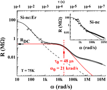
To fabricate practical light-emitting devices, identification and minimization of nonradiative processes are necessary. In this study, an electrical measurement technique for time-resolved analyses of nonradiative processes was proposed. From the comparison between a commercial light-emitting diode (LED) and rare-earth-doped semiconductors, the technique, called electrical frequency-response analysis (FRA), revealed differences in the charge behaviors in the pn junction of bulk semiconductors and impurities. Although the charge response time constant on the order of a nanosecond realized effective recombination of the electron–hole pairs in a LED, the time constant larger than a microsecond still limited the emission intensity of the rare-earth-doped semiconductors such as Er-doped Si nanocrystals and GaAs with Er and O codopants. The energy-loss processes of the Er-doped semiconductors were investigated, and countermeasures to enhance the emission intensity were proposed.

Type
Invited Feature Papers
Copyright
Copyright © Materials Research Society 2014 

Access options

Get access to the full version of this content by using one of the access options below. (Log in options will check for institutional or personal access. Content may require purchase if you do not have access.)

Footnotes

This paper has been selected as an Invited Feature Paper.

References

REFERENCES

Pomrenke, G.S., Ennen, H., and Haydl, W.: Photoluminescence optimization and characteristics of the rare-earth element erbium implanted in GaAs, InP, and GaP. J. Appl. Phys. 59, 601 (1986).CrossRefGoogle Scholar
Bantien, F., Bauser, E., and Weber, J.: Incorporation of erbium in GaAs by liquid-phase epitaxy. J. Appl. Phys. 61, 2803 (1987).Google Scholar
Uwai, K., Nakagome, H., and Takahei, K.: Er-doped InP and GaAs grown by metalorganic chemical vapor deposition. Appl. Phys. Lett. 51, 1010 (1987).CrossRefGoogle Scholar
Namavar, F., Lu, F., Perry, C.H., Cremins, A., Kalkhoran, N.M., and Soref, R.A.: Strong room-temperature infrared emission from Er-implanted porous Si. J. Appl. Phys. 77, 4813 (1995).CrossRefGoogle Scholar
Minissale, S., Vinh, N.Q., de Boer, W., Bresler, M.S., and Gregorkiewicz, T.: Microscopic evidence for role of oxygen in luminescence of Er3+ ions in Si: Two-color and pump-probe spectroscopy. Phys. Rev. B 78, 035313 (2008).CrossRefGoogle Scholar
Taguchi, A., Takahei, K., and Horikoshi, Y.: Multiphonon-assisted energy transfer between Yb 4f shell and InP host. J. Appl. Phys. 76, 7288 (1994).CrossRefGoogle Scholar
Hogg, R.A., Takahei, K., and Taguchi, A.: Er-related trap levels in GaAs:Er, O studied by optical spectroscopy under hydrostatic pressure. Phys. Rev. B 56, 10255 (1997).Google Scholar
Taguchi, A. and Takahei, K.: Erbium in Si: Estimation of energy transfer rate and trap depth from temperature dependence of intra-4f-shell luminescence. J. Appl. Phys. 83, 2800 (1998).Google Scholar
Elsaesser, D.W., Yeo, Y.K., Hengehold, R.L., Evans, K.R., and Pedrotti, F.L.: Er related deep centers in GaAs doped with Er by ion implantation and molecular beam epitaxy. J. Appl. Phys. 77, 3919 (1995).CrossRefGoogle Scholar
Song, S.F., Chen, W.D., Zhang, C., Bian, L., Hsu, C.C., Lu, L.W., Zhang, Y.H., and Zhu, J.: Electrical characterization of Er- and Pr-implanted GaN films. Appl. Phys. Lett. 86, 152111 (2005).CrossRefGoogle Scholar
Mamor, M., Pipeleers, B., Auret, F.D., and Vantomme, A.: Defect production in strained p-type Si1-xGex by Er implantation. J. Appl. Phys. 109, 013715 (2011).Google Scholar
Ishii, M., Towlson, B., Harako, S., Zhao, X., Komuro, S., and Hamilton, B.: Charge propagation dynamics in temperature quenching of Sm-doped TiO2: Impedance spectroscopy of release processes of trapped charges determining luminescence intensity. Jpn. J. Appl. Phys. 52, 025601 (2013).Google Scholar
Ishii, M., Crowe, I., Halsall, M., Knights, A., Gwilliam, R., and Hamilton, B.: Investigation of the thermal charge ‘trapping-detrapping’ in silicon nanocrystals: Correlation of the optical properties with complex impedance spectra. Appl. Phys. Lett. 101, 242108 (2012).Google Scholar
Han, J., Senos, A.M.R., Mantas, P.Q., and Cao, W.: Dielectric relaxation of shallow donor in polycrystalline Mn-doped ZnO. J. Appl. Phys. 93, 4097 (2003).CrossRefGoogle Scholar
Ishii, M., Harako, S., Zhao, X., Komuro, S., and Hamilton, B.: Charge propagation dynamics at trapping centers that induce the luminescence of rare-earth dopants in wide-gap materials. Appl. Phys. Lett. 99, 101909 (2011).CrossRefGoogle Scholar
Crowe, I.F., Kashtiban, R.J., Sherliker, B., Bangert, U., Halsall, M.P., Knights, A.P., and Gwilliam, R.M.: Photoluminescence from SiO2 films containing Si nanocrystals and Er: Effects of nanocrystalline size on the photoluminescence efficiency of Er3+ . J. Appl. Phys. 84, 4525 (1998).Google Scholar
Crowe, I.F., Halsall, M.P., Hulko, O., Knights, A.P., Gwilliam, R.M., Wojdak, M., and Kenyon, A.J.: Probing the phonon confinement in ultrasmall silicon nanocrystals reveals a size-dependent surface energy. J. Appl. Phys. 109, 083534 (2011).CrossRefGoogle Scholar
Fujiwara, Y., Furuta, S., Makita, K., Ito, Y., Nonogaki, Y., and Takeda, Y.: Drastic effects of hydrogen flow rate on growth characteristics and electrical/optical properties of InP grown by organometallic vapour phase epitaxy with TMIn and TBP. J. Cryst. Growth 146, 544 (1995).Google Scholar
Uren, M.J., Stathis, J.H., and Cartier, E.: Conductance measurements on Pb centers at the (111) Si:SiO2 interface. J. Appl. Phys. 80, 3915 (1996).Google Scholar
Koizumi, A., Fujiwara, Y., Inoue, K., Urakami, A., Yoshikane, T., and Takeda, Y.: Room-temperature 1.54 μm light emission from Er,O-codoped GaAs/GaInP light-emitting diodes grown by low-pressure organometallic vapor phase epitaxy. Jpn. J. Appl. Phys. 42, 2223 (2003).CrossRefGoogle Scholar
Takahei, K. and Taguchi, A.: Selective formation of an efficient ErO luminescence center in GaAs by metalorganic chemical vapor deposition under an atmosphere containing oxygen. J. Appl. Phys. 74, 1979 (1993).Google Scholar
Hogg, R., Takahei, K., Taguchi, A., and Horikoshi, Y.: Preferential alignment of Er–2O centers in GaAs:Er, O revealed by anisotropic host excited photoluminescence. Appl. Phys. Lett. 68, 3317 (1996).CrossRefGoogle Scholar
Ishii, M., Crowe, I., Halsall, M., Knights, A., Gwilliam, R., and Hamilton, B.: Electrical observation of non-radiative recombination in Er doped Si nano-crystals during thermal quenching of intra-4f luminescence. Jpn. J. Appl. Phys. 53, 031302 (2014).CrossRefGoogle Scholar
Barsoukov, E. and Macdonald, J.R.: Impedance Spectroscopy Theory, Experiment, and Applications (John Wiley and Sons, Inc., New Jersey, 2005), p. 30.Google Scholar
Ishii, M., Koizumi, A., Takeda, Y., and Fujiwara, Y.: Discrimination of energy transfer and back transfer between GaAs host and Er luminescent dopants using electric response analysis. J. Appl. Phys. 115, 133510 (2014).Google Scholar