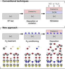
Crossref Citations
This article has been cited by the following publications. This list is generated based on data provided by
Crossref.
Rozen, John
Ahyi, Ayayi C.
Zhu, Xingguang
Williams, John R.
and
Feldman, Leonard C.
2011.
Scaling Between Channel Mobility and Interface State Density in SiC MOSFETs.
IEEE Transactions on Electron Devices,
Vol. 58,
Issue. 11,
p.
3808.
Pitthan, E.
Gobbi, A.L.
Boudinov, H.I.
and
Stedile, F.C.
2015.
SiC Nitridation by NH3 Annealing and Its Effects in MOS Capacitors with Deposited SiO2 Films.
Journal of Electronic Materials,
Vol. 44,
Issue. 8,
p.
2823.
Chanthaphan, Atthawut
Hosoi, Takuji
Shimura, Takayoshi
and
Watanabe, Heiji
2015.
Study of SiO2/4H-SiC interface nitridation by post-oxidation annealing in pure nitrogen gas.
AIP Advances,
Vol. 5,
Issue. 9,
Siddiqui, Amna
Elgabra, Hazem
and
Singh, Shakti
2016.
Surface passivation method for optimum performance of 4H-SiC devices.
p.
1.
Siddiqui, Amna
Elgabra, Hazem
and
Singh, Shakti
2016.
The Current Status and the Future Prospects of Surface Passivation in 4H-SiC Transistors.
IEEE Transactions on Device and Materials Reliability,
Vol. 16,
Issue. 3,
p.
419.
Peng, Zhao Yang
Wang, Yi Yu
Shen, Hua Jun
Bai, Yun
Tang, Yi Dan
Chen, Xi Ming
Li, Cheng Zhan
Liu, Ke An
and
Liu, Xin Yu
2017.
Re-Investigation of SiC/SiO<sub>2</sub> Interface Passivation by Nitrogen Annealing.
Materials Science Forum,
Vol. 897,
Issue. ,
p.
335.
Pitthan, E.
Amarasinghe, V.P.
Xu, C.
Gustafsson, T.
Stedile, F.C.
and
Feldman, L.C.
2017.
4H-SiC surface energy tuning by nitrogen up-take.
Applied Surface Science,
Vol. 402,
Issue. ,
p.
192.
Sun, Qiu-Jie
Zhang, Yu-Ming
Song, Qing-Wen
Tang, Xiao-Yan
Zhang, Yi-Meng
Li, Cheng-Zhan
Zhao, Yan-Li
and
Zhang, Yi-Men
2017.
Near-interface oxide traps in 4H–SiC MOS structures fabricated with and without annealing in NO.
Chinese Physics B,
Vol. 26,
Issue. 12,
p.
127701.
Mori, Daisuke
Fujita, Yoshiki
Hirose, Takayuki
Murata, Koichi
Tsuchida, Hidekazu
and
Matsui, Fumihiko
2018.
Atomic characterization of nano-facet nitridation at SiC (11¯00) surface.
Applied Physics Letters,
Vol. 112,
Issue. 13,
Kwon, Sera
Kim, Dae-Kyoung
Cho, Mann-Ho
and
Chung, Kwun-Bum
2018.
Reduction of defect states in atomic-layered HfO2 film on SiC substrate using post-nitridation annealing.
Thin Solid Films,
Vol. 645,
Issue. ,
p.
102.
Tang, Guannan
Tang, Xiaoyan
Zhang, Yuming
Yifan
Jia
Zhang, Yimen
and
Song, Qingwen
2018.
Study of the SiO2/4H-SiC Interface Obtained by Oxidation of Nitrogen Doped Nanoscale Epitaxial Layer.
p.
233.
Liu, Xinyu
Hao, Jilong
You, Nannan
Bai, Yun
and
Wang, Shengkai
2019.
High-pressure microwave plasma oxidation of 4H-SiC with low interface trap density.
AIP Advances,
Vol. 9,
Issue. 12,
Liu, Xin-Yu
Hao, Ji-Long
You, Nan-Nan
Bai, Yun
Tang, Yi-Dan
Yang, Cheng-Yue
and
Wang, Sheng-Kai
2020.
High-mobility SiC MOSFET with low density of interface traps using high pressure microwave plasma oxidation*.
Chinese Physics B,
Vol. 29,
Issue. 3,
p.
037301.
Murata, Koichi
Mori, Daisuke
Tsuji, Hidenori
Fujii, Takeshi
Takigawa, Aki
and
Tsuchida, Hidekazu
2020.
Direct nitridation of 4H-SiC(0001) surface by H2/N2 treatment.
Applied Physics Express,
Vol. 13,
Issue. 9,
p.
095506.
Jayawardhena, I. U.
Ramamurthy, R. P.
Morisette, D.
Ahyi, A. C.
Thorpe, R.
Kuroda, M. A.
Feldman, L. C.
and
Dhar, S.
2021.
Effect of surface treatments on ALD Al2O3/4H-SiC metal–oxide–semiconductor field-effect transistors.
Journal of Applied Physics,
Vol. 129,
Issue. 7,
Siddiqui, Amna
Khosa, Rabia Yasmin
and
Usman, Muhammad
2021.
High-kdielectrics for 4H-silicon carbide: present status and future perspectives.
Journal of Materials Chemistry C,
Vol. 9,
Issue. 15,
p.
5055.
Wang, Ying
He, Yanjing
Tang, Xiaoyan
Song, Qingwen
Li, Dongxun
Yuan, Hao
Gong, Xiaowu
and
Zhang, Yuming
2023.
Effects of 5 MeV proton irradiation on 4H-SiC lateral pMOSFETs on-state characteristics.
Microelectronics Journal,
Vol. 137,
Issue. ,
p.
105799.
Ke, Chengxuan
Nie, Chenxi
and
Luo, Guangfu
2023.
High-temperature effects for transition state calculations in solids.
The Journal of Chemical Physics,
Vol. 159,
Issue. 20,


