Hostname: page-component-8448b6f56d-t5pn6 Total loading time: 0 Render date: 2024-04-24T00:41:13.765Z Has data issue: false hasContentIssue false

Improved structural and electrical properties of thin ZnO:Al films by dc filtered cathodic arc deposition

Published online by Cambridge University Press:  07 November 2011

Yuankun Zhu*
Affiliation:
Harbin Institute of Technology, Harbin 150080, People’s Republic of China; and Lawrence Berkeley National Laboratory, Plasma Applications Group, Berkeley, California 94720
Rueben J. Mendelsberg
Affiliation:
Lawrence Berkeley National Laboratory, Plasma Applications Group, Berkeley, California 94720; and Lawrence Berkeley National Laboratory, Molecular Foundry, Berkeley, California 94720
Sunnie H.N. Lim
Affiliation:
Lawrence Berkeley National Laboratory, Plasma Applications Group, Berkeley, California 94720
Jiaqi Zhu
Affiliation:
Harbin Institute of Technology, Harbin 150080, People’s Republic of China
Jiecai Han
Affiliation:
Harbin Institute of Technology, Harbin 150080, People’s Republic of China
André Anders
Affiliation:
Lawrence Berkeley National Laboratory, Plasma Applications Group, Berkeley, California 94720
*
a)Address all correspondence to this author. e-mail: yuan.kun.zhu@gmail.com
Get access

Abstract

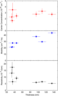
Transparent conducting oxide films are usually several 100-nm thick to achieve the required low sheet resistance. In this study, we show that the filtered cathodic arc technique produces high-quality low-cost ZnO:Al material for comparably smaller thicknesses than achieved by magnetron sputtering, making arc deposition a promising choice for applications requiring films less than 100-nm thick. A mean surface roughness less than 1 nm is observed for ZnO:Al films less than 100-nm thick, and 35-nm-thick ZnO:Al films exhibit Hall mobility of 28 cm2/Vs and a low resistivity of 6.5 × 10⁻⁴ Ωcm. Resistivity as low as 5.2 × 10⁻⁴ Ωcm and mobility as high as 43.5 cm2/Vs are obtained for 135-nm films.

Type
Articles
Copyright
Copyright © Materials Research Society 2011

Access options

Get access to the full version of this content by using one of the access options below. (Log in options will check for institutional or personal access. Content may require purchase if you do not have access.)

References

REFERENCES

1.Liu, H., Avrutin, V., Izyumskaya, N., Özgür, Ü., and Morkoç, H.: Transparent conducting oxides for electrode applications in light emitting and absorbing devices. Superlattices Microstruct. 48(5), 458 (2010).CrossRefGoogle Scholar
2.Kim, H., Horwitz, J.S., Kushto, G., Piqué, A., Kafafi, Z.H., Gilmore, C.M., and Chrisey, D.B.: Effect of film thickness on the properties of indium tin oxide thin films. J. Appl. Phys. 88(10), 6021 (2000).CrossRefGoogle Scholar
3.Kumar, K.J., Raju, N.R.C., and Subrahmanyam, A.: Thickness dependent physical and photocatalytic properties of ITO thin films prepared by reactive DC magnetron sputtering. Appl. Surf. Sci. 257(7), 3075 (2011).CrossRefGoogle Scholar
4.Amanullah, F.M., Pratap, K.J., and Babu, V.H.: Thickness dependence of electrical and structural properties of FTO films. Cryst. Res. Technol. 26, 1099 (1991).CrossRefGoogle Scholar
5.Moholkar, A.V., Pawar, S.M., Rajpure, K.Y., Patil, P.S., and Bhosale, C.H.: Properties of highly oriented spray-deposited fluorine-doped tin oxide thin films on glass substrates of different thickness. J. Phys. Chem. Solids 68(10), 1981 (2007).CrossRefGoogle Scholar
6.Rakhshani, A., Makdisi, Y., and Ramazaniyan, H.: Electronic and optical properties of fluorine-doped tin oxide films. J. Appl. Phys. 83(2), 1049 (1998).CrossRefGoogle Scholar
7.Fortunato, E., Gonçalves, A., Assunção, V., Marques, A., Águas, H., Pereira, L., Ferreira, I., and Martins, R.: Growth of ZnO:Ga thin films at room temperature on polymeric substrates: Thickness dependence. Thin Solid Films 442(1–2), 121 (2003).CrossRefGoogle Scholar
8.Minami, T.: Transparent conducting oxide semiconductors for transparent electrodes. Semicond. Sci. Technol. 20(4), S35 (2005).CrossRefGoogle Scholar
9.Dong, B-Z., Fang, G-J., Wang, J-F., Guan, W-J., and Zhao, X-Z.: Effect of thickness on structural, electrical, and optical properties of ZnO: Al films deposited by pulsed laser deposition. J. Appl. Phys. 101(3), 033713 (2007).CrossRefGoogle Scholar
10.Anders, A., Lim, S.H.N., Yu, K.M., Andersson, J., Rosén, J., McFarland, M., and Brown, J.: High quality ZnO:Al transparent conducting oxide films synthesized by pulsed filtered cathodic arc deposition. Thin Solid Films 518, 3313 (2010).CrossRefGoogle Scholar
11.Liang, G-X., Fan, P., Cai, X-M., Zhang, D-P., and Zheng, Z-H.: The influence of film thickness on the transparency and conductivity of al-doped ZnO thin films fabricated by ion-beam sputtering. J. Electron. Mater. 40(3), 267 (2011).CrossRefGoogle Scholar
12.Lee, H-C. and Ok Park, O.: The evolution of the structural, electrical and optical properties in indium-tin-oxide thin film on glass substrate by DC reactive magnetron sputtering. Vacuum 80(8), 880 (2006).CrossRefGoogle Scholar
13.Agashe, C., Kluth, O., Hupkes, J., Zastrow, U., Rech, B., and Wuttig, M.: Efforts to improve carrier mobility in radio frequency sputtered aluminum doped zinc oxide films. J. Appl. Phys. 95(4), 1911 (2004).CrossRefGoogle Scholar
14.Bai, S.N. and Tseng, T.Y.: Effect of alumina doping on structural, electrical, and optical properties of sputtered ZnO thin films. Thin Solid Films 515(3), 872 (2006).CrossRefGoogle Scholar
15.Cebulla, R., Wendt, R., and Ellmer, K.: Al-doped zinc oxide films deposited by simultaneous rf and dc excitation of a magnetron plasma: Relationships between plasma parameters and structural and electrical film properties. J. Appl. Phys. 83(2), 1087 (1998).CrossRefGoogle Scholar
16.Ellmer, K., Kudella, F., Mientus, R., Schieck, R., and Fiechter, S.: Influence of discharge parameters on the layer properties of reactive magnetron sputtered ZnO:Al films. Thin Solid Films 247(1), 15 (1994).CrossRefGoogle Scholar
17.Fang, G., Li, D., and Yao, B-L.: Fabrication and characterization of c-axis-oriented transparent conductive nanocrystalline AZO thin films by rf magnetron sputtering. Proc. SPIE 4919, 405 (2002).CrossRefGoogle Scholar
18.Hoon, J-W., Chan, K-Y., Krishnasamy, J., Tou, T-Y., and Knipp, D.: Direct current magnetron sputter-deposited ZnO thin films. Appl. Surf. Sci. 257(7), 2508 (2011).CrossRefGoogle Scholar
19.Jäger, S., Szyszka, B., Szczyrbowski, J., and Bräuer, G.: Comparison of transparent conductive oxide thin films prepared by a.c. and d.c. reactive magnetron sputtering. Surf. Coat. Tech. 98(1–3), 1304 (1998).CrossRefGoogle Scholar
20.Maniv, S., Westwood, W., and Colombini, E.: Pressure and angle of incidence effects in reactive planar magnetron sputtered ZnO layers. J. Vac. Sci. Technol. 20(2), 162 (1982).CrossRefGoogle Scholar
21.Szyszka, B.: Transparent and conductive aluminum doped zinc oxide films prepared by mid-frequency reactive magnetron sputtering. Thin Solid Films 351, 164 (1999).CrossRefGoogle Scholar
22.Tominaga, K., Umezu, N., Mori, I., Ushiro, T., Moriga, T., and Nakabayashi, I.: Transparent conductive ZnO film preparation by alternating sputtering of ZnO:Al and Zn or Al targets. Thin Solid Films 334(1–2), 35 (1998).CrossRefGoogle Scholar
23.Di Trolio, A., Bauer, E.M., Scavia, G., and Veroli, C.: Blueshift of optical band gap in c-axis oriented and conducting Al-doped ZnO thin films. J. Appl. Phys. 105(11), 113109 (2009).CrossRefGoogle Scholar
24.Park, S-M., Ikegami, T., and Ebihara, K.: Investigation of transparent conductive oxide Al-doped ZnO films produced by pulsed laser deposition. Jpn. J. Appl. Phys. 44(11), 8027 (2005).CrossRefGoogle Scholar
25.Prasad, S., Nainaparampil, J., and Zabinski, J.: Tribological behavior of alumina doped zinc oxide films grown by pulsed laser deposition. J. Vac. Sci. Technol., A 20(5), 1738 (2002).CrossRefGoogle Scholar
26.Suzuki, A., Matsushita, T., Wada, N., Sakamoto, Y., and Okuda, M.: Transparent conducting Al-doped ZnO thin films prepared by pulsed laser deposition. Jpn. J. Appl. Phys. 35, L56 (1996).CrossRefGoogle Scholar
27.Suzuki, A., Nakamura, M., Michihata, R., Aoki, T., Matsushita, T., and Okuda, M.: Ultrathin Al-doped transparent conducting zinc oxide films fabricated by pulsed laser deposition. Thin Solid Films 517(4), 1478 (2008).CrossRefGoogle Scholar
28.Tanaka, H., Ihara, K., Miyata, T., Sato, H., and Minami, T.: Low resistivity polycrystalline ZnO:Al thin films prepared by pulsed laser deposition. J. Vac. Sci. Technol., A 22(4), 1757 (2004).CrossRefGoogle Scholar
29.Tay, B.K., Zhao, Z.W., and Chua, D.H.C.: Review of metal oxide films deposited by filtered cathodic vacuum arc technique. Mater. Sci. Eng., R 52(1–3), 1 (2006).CrossRefGoogle Scholar
30.Goldsmith, S.: Filtered vacuum arc deposition of undoped and doped ZnO thin films: Electrical, optical, and structural properties. Surf. Coat. Tech. 201(7), 3993 (2006).CrossRefGoogle Scholar
31.Lee, H.W., Lau, S.P., Wang, Y.G., Tse, K.Y., Hng, H.H., and Tay, B.K.: Structural, electrical and optical properties of Al-doped ZnO thin films prepared by filtered cathodic vacuum arc technique. J. Cryst. Growth 268(3–4), 596 (2004).CrossRefGoogle Scholar
32.Mendelsberg, R.J., Lim, S.H.N., Zhu, Y.K., Wallig, J., Milliron, D.J., and Anders, A.: Achieving high mobility ZnO:Al at very high growth rates by dc filtered cathodic arc deposition. J. Phys. D: Appl. Phys. 44(23), 232003 (2011).CrossRefGoogle Scholar
33.Zhitomirsky, V.N., Çetinörgü, E., Adler, E., Rosenberg, Y., Boxman, R.L., and Goldsmith, S.: Filtered vacuum arc deposition of transparent conducting Al-doped ZnO films. Thin Solid Films 515(3), 885 (2006).CrossRefGoogle Scholar
34.Anders, A.: Atomic scale heating in cathodic arc plasma deposition. Appl. Phys. Lett. 80(6), 1100 (2002).CrossRefGoogle Scholar
35.Anders, A.: Energetic deposition using filtered cathodic arc plasmas. Vacuum 67, 673 (2002).CrossRefGoogle Scholar
36.Anders, A.: Approaches to rid cathodic arc plasma of macro- and nanoparticles: A review. Surf. Coat. Tech. 120121, 319 (1999).CrossRefGoogle Scholar
37.Anders, A.: Cathodic Arcs: From Fractal Spots to Energetic Condensation (Springer, New York, 2008).CrossRefGoogle Scholar
38.Anders, A. and Kühn, M.: Characterization of a low-energy constricted-plasma source. Rev. Sci. Instrum. 69(3), 1340 (1998).CrossRefGoogle Scholar
39.Jin, Z-C., Hamberg, I., and Granqvist, C.G.: Optical properties of sputter-deposited ZnO:Al thin films. J. Appl. Phys. 64(10), 5117 (1988).CrossRefGoogle Scholar
40.Petrov, I., Barna, P.B., Hultman, L., and Greene, J.E.: Microstructural evolution during film growth. J. Vac. Sci. Technol., A 21(5), S117 (2003).CrossRefGoogle Scholar
41.Betz, U., Olsson, M.K., Marthy, J., and Escolá, M.F.: On the synthesis of ultra smooth ITO thin films by conventional direct current magnetron sputtering. Thin Solid Films 516(7), 1334 (2008).CrossRefGoogle Scholar
42.Klöppel, A., Kriegseis, W., Meyer, B.K., Scharmann, A., Daube, C., Stollenwerk, J., and Trube, J.: Dependence of the electrical and optical behaviour of ITO-silver-ITO multilayers on the silver properties. Thin Solid Films 365, 139 (2000).CrossRefGoogle Scholar
43.Kuriki, S. and Kawashima, T.: Mechanical properties of Al2O3-doped (2 wt.%) ZnO films. Thin Solid Films 515(24), 8594 (2007).CrossRefGoogle Scholar
44.Chang, H.P., Wang, F.H., Wu, J.Y., Kung, C.Y., and Liu, H.W.: Enhanced conductivity of aluminum doped ZnO films by hydrogen plasma treatment. Thin Solid Films 518(24), 7445 (2010).CrossRefGoogle Scholar
45.Konishi, R., Noda, K., Harada, H., and Sasakura, H.: The preparation of transparent ZnO: Al thin films. J. Cryst. Growth 117(1–4), 939 (1992).CrossRefGoogle Scholar
46.Lee, H.W., Lau, S.P., Wang, Y.G., Tay, B.K., and Hng, H.H.: Internal stress and surface morphology of zinc oxide thin films deposited by filtered cathodic vacuum arc technique. Thin Solid Films 458(1–2), 15 (2004).CrossRefGoogle Scholar
47.Agura, H., Suzuki, A., Matsushita, T., Aoki, T., and Okuda, M.: Low resistivity transparent conducting Al-doped ZnO films prepared by pulsed laser deposition. Thin Solid Films 445(2), 263 (2003).CrossRefGoogle Scholar
48.Kim, H., Piqué, A., Horwitz, J.S., Murata, H., Kafafi, Z.H., Gilmore, C.M., and Chrisey, D.B.: Effect of aluminum doping on zinc oxide thin films grown by pulsed laser deposition for organic light-emitting devices. Thin Solid Films 377378, 798 (2000).CrossRefGoogle Scholar
49.Ghafoor, N., Eriksson, F., Persson, P.O.Å., Hultman, L., and Birch, J.: Effects of ion-assisted growth on the layer definition in Cr/Sc multilayers. Thin Solid Films 516(6), 982 (2008).CrossRefGoogle Scholar
50.Tungasmita, S., Persson, P., Hultman, L., and Birch, J.: Pulsed low-energy ion-assisted growth of epitaxial aluminum nitride layer on 6H-silicon carbide by reactive magnetron sputtering. J. Appl. Phys. 91(6), 3551 (2002).CrossRefGoogle Scholar