Hostname: page-component-76fb5796d-dfsvx Total loading time: 0 Render date: 2024-04-25T10:29:14.643Z Has data issue: false hasContentIssue false

Understanding the effect of impurities and grain boundaries on mechanical behavior of Si via nanoindentation of (110)/(100) direct Si bonded wafers

Published online by Cambridge University Press:  27 September 2011

Khaled Youssef*
Affiliation:
Department of Material Science and Engineering, North Carolina State University, Raleigh, North Carolina 27606
Xuegong Yu
Affiliation:
Department of Materials Science Engineering and State Key Lab of Silicon Materials, Zhejiang University, 310027 Hangzhou, People’s Republic of China
Mike Seacrist
Affiliation:
MEMC Electronic Materials, Inc., St. Peters, Missouri 63376
George Rozgonyi
Affiliation:
Department of Material Science and Engineering, North Carolina State University, Raleigh, North Carolina 27606
*
a)Address all correspondence to this author. e-mail: khaled_youssef@ncsu.edu
Get access

Abstract

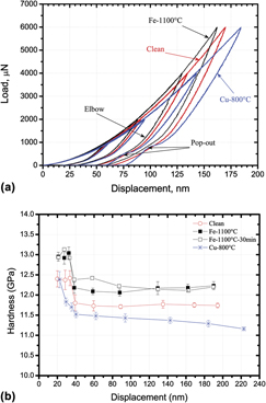
Nanoindentation was used to examine the impact of impurities and grain boundaries on the mechanical properties of a “model” (110)/(100) grain boundary (GB) interface prepared using direct silicon bonding via the hybrid orientation technique of (110) and (100) p-type silicon wafers. Remarkable differences were found between the mechanical behavior of Fe- and Cu-contaminated samples. The direct silicon bonded wafers contaminated with either Fe or Cu showed opposite effects on mechanical properties, with Fe enhancing the silicon hardness, while Cu contamination induces a gradual weakening. High-resolution transmission electron microscopy was used to verify that the abrupt hardness changes observed during increasing nanoindentation loading is attributed to local deformation induced by the GB interface, Cu precipitate colony induced dislocations, and the abrupt crystallographic orientation change across the GB. The resulting dislocation loop generation facilitated the deformation process during nanoindentation and therefore softened the material.

Type
Articles
Copyright
Copyright © Materials Research Society 2011

Access options

Get access to the full version of this content by using one of the access options below. (Log in options will check for institutional or personal access. Content may require purchase if you do not have access.)

References

REFERENCES

1.Yonenaga, I. and Sumino, K.: Mechanical strength of silicon crystals as a function of the oxygen concentration. J. Appl. Phys. 56, 2346 (1984).CrossRefGoogle Scholar
2.Spitznagel, A., Seidensticker, R.G., Lien, S.Y., and Hopkins, R.H., in: Oxygen, Carbon, Hydrogen, and Nitrogen in Silicon, Mater. Res. Soc. Symp. Proc., Eds. Mikkelsen, J.C., Pearton, S.J., Corbett, J.W., and Pennycook, S.J.. Pennington, NJ, 383 (1986).Google Scholar
3.Shimura, F. and Hockett, R.S.: Nitrogen effect on oxygen precipitation in Czochralski silicon. Appl. Phys. Lett. 48, 224 (1986).CrossRefGoogle Scholar
4.Ge, D., Minor, A.M., Stach, E.A., and Morris, J.W. Jr.: Size effects in the nanoindentation of silicon at ambient temperature. Phil Mag. 86, 4069 (2006).CrossRefGoogle Scholar
5.Sumino, K., Yonenaga, I., Imai, M., and Abe, T.: Effects of nitrogen on dislocation behavior and mechanical strength in silicon crystals. J. Appl. Phys. 54, 5016 (1983).CrossRefGoogle Scholar
6.Hu, S.M. and Patrick, W.J.: Effect of oxygen on dislocation movement in silicon. J. Appl. Phys. 46, 1869 (1975).CrossRefGoogle Scholar
7.Murphy, J.D., Giannattasio, A., Alpass, C.R., Senkader, S., Falster, R.J., and Wilshaw, P.R.: The influence of nitrogen on dislocation locking in float-zone silicon. Solid State Phenom. 108109, 139 (2005).CrossRefGoogle Scholar
8.Yang, M., Chan, W.C., Chan, K.K., Shi, L., Fried, D.M., Stathis, J.H., Chou, A.I., Gusev, E., Ott, J.A., Burns, L.E., Fischetti, M.V., and Ieong, M.: Hybrid-orientation technology (HOT): Opportunities and challenges. IEEE Trans. Elec. Dev., 53, 965 (2006).CrossRefGoogle Scholar
9.Pharr, G.M.: Measurements of mechanical properties by ultra-low load indentation. Mater. Sci. Eng. A253, 151 (1998).CrossRefGoogle Scholar
10.Oliver, W.C. and Pharr, G.M.: An improved technique for determining hardness and elastic modulus using load and displacement sensing indentation experiments. J. Mater. Res. 7, 1564 (1992).CrossRefGoogle Scholar
11.Doerner, M.F. and Nix, W.D.: A method for interpreting the data from depth-sensing indentation instruments. J. Mater. Res. 1, 601 (1986).CrossRefGoogle Scholar
12.Chasiotis, I., Cho, S.W., and Jonnalagadda, K.: Fracture toughness and subcritical crack growth in polycrystalline silicon. Trans. ASME 73, 714 (2006).CrossRefGoogle Scholar
13.Lawn, B.R., Marshall, D.B., Anstis, G.R., and Dabbs, T.P.: Fatigue analysis of brittle materials using indentation flaws. J. Mater. Sci. 16, 2846 (1981).CrossRefGoogle Scholar
14.Lawn, B. and Wilshaw, R.: Indentation fracture: Principles and applications. J. Mater. Sci. 10, 1049 (1975).CrossRefGoogle Scholar
15.Oliver, W.C. and Pharr, G.M.: Measurement of hardness and elastic modulus by instrumented indentation: Advances in understanding and refinements to methodology. J. Mater. Res. 19, 3 (2004).CrossRefGoogle Scholar
16.Cheng, Y. and Cheng, C.: Further analysis of indentation loading curves: Effects of tip rounding on mechanical property measurements. J. Mater. Res. 13, 1059 (1998).CrossRefGoogle Scholar
17.Rozgonyi, G., Lu, J., Wagener, M., Yu, X., Park, Y., and Youssef, K.: Enhancing Silicon PV Materials Research via IC Wafer Engineering Defect Science Experiences and Industry/University Consortia: SiWEDS to SiSoC. The 5th Inter. Sympo. Adv. Sci. Tech. Si Mater. Nov. (2008), 323, Hawaii, USA.Google Scholar
18.Ebrahimi, F. and Kalwani, L.: Fracture anisotropy in silicon single crystal. Mater. Sci. Eng. A268, 116 (1999).CrossRefGoogle Scholar
19.Lawn, B.R. and Swain, M.V.: Microfracture beneath point indentations in brittle solids. J. Mater. Sci. 10, 113 (1975).CrossRefGoogle Scholar
20.Shikimaka, O. and Grabco, D.: Deformation created by Berkovich and Vickers indenters and its influence on surface morphology of indentations for LiF and CaF2 single crystals. J. Phys. D: Appl. Phys. 41, 074012 (2008).CrossRefGoogle Scholar
21.Chen, J. and Bull, S.J.: On the relationship between plastic zone radius and maximum depth during nanoindentation. Surf. Coat. Tech. 201, 4289 (2006).CrossRefGoogle Scholar
22.Jang, J., Lance, M.J., Wen, S., Tsui, T.Y., and Pharr, G.M.: Indentation-induced phase transformations in silicon: influences of load, rate and indenter angle on the transformation behavior. Acta Mater. 53, 1759 (2005).CrossRefGoogle Scholar
23.Domnich, V., Gogotsi, Y., and Dub, S.: Effect of phase transformations on the shape of the unloading curve in the nanoindentation of silicon. Appl. Phys. Lett. 76, 2214 (2000).CrossRefGoogle Scholar
24.Weber, E.R.: Transition metals in silicon. Appl. Phys. A30, 1 (1983).CrossRefGoogle Scholar
25.Seibt, M., Griess, M., Istratov, A.A., Hedemann, H., Sattler, A., and Schroter, W.: Formation and properties of copper silicide precipitates in silicon. Phys. Stat. Sol., 166, 177 (1998).3.0.CO;2-2>CrossRefGoogle Scholar
26.Dash, W.C.: Copper precipitation on dislocations in silicon. J. Appl. Phys. 27, 1193 (1956).CrossRefGoogle Scholar
27.Gottschalk, H.: Precipitation of copper silicide on glide dislocations in silicon at low temperature. Phys. Stat. Sol. 137, 447 (1993).CrossRefGoogle Scholar
28.Xi, Z., Yang, D., Chen, J., Xu, J., Ji, Y., Que, D., and Moeller, H.: Influence of copper precipitation on oxygen precipitation in Czochralski silicon. Semicond. Sci. Tech. 19, 299 (2004).CrossRefGoogle Scholar
29.Broniatowski, A. and Haut, C.: The electronic properties of copper-decorated twinned boundaries in silicon. Phil. Mag. Lett. 62, 407 (1990).CrossRefGoogle Scholar
30.Seibt, M.: On the role of stacking-faults in copper precipitation in silicon. Sol. Stat. Phenom., 1920, 45 (1991).CrossRefGoogle Scholar