Hostname: page-component-8448b6f56d-dnltx Total loading time: 0 Render date: 2024-04-20T04:22:58.133Z Has data issue: false hasContentIssue false

Surface-induced effects in GaN nanowires

Published online by Cambridge University Press:  15 August 2011

Raffaella Calarco
Affiliation:
Paul-Drude-Institut für Festkörperelektronik, 10117 Berlin, Germany
Toma Stoica
Affiliation:
Peter Grünberg Institut (PGI-9), Forschungszentrum Jülich, D-52425 Jülich, Germany; and Jülich-Aachen Research Alliance, D-52425 Jülich, Germany
Oliver Brandt
Affiliation:
Paul-Drude-Institut für Festkörperelektronik, 10117 Berlin, Germany
Lutz Geelhaar*
Affiliation:
Paul-Drude-Institut für Festkörperelektronik, 10117 Berlin, Germany
*
a)Address all correspondence to this author. e-mail: geelhaar@pdi-berlin.de
Get access

Abstract

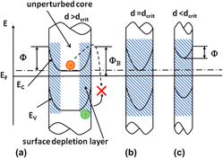
Semiconductor nanowires (NWs) are characterized by an extraordinarily large surface-to-volume ratio. Consequently, surface effects are expected to play a much larger role than in thin films. Here, we review a research focused on the impact of the surface on the electrical and optical properties of catalyst-free GaN NWs with growth direction <0001>. Using a combination of complementary experimental techniques, it has been shown that the Fermi level is pinned at the NW sidewall surfaces, resulting in internal electric fields and in full depletion for NWs below a critical diameter. Deoxidation of the surfaces unpins the Fermi level, leading to enhanced radiative recombination of excitons. Prominent absorption below the bandgap is caused by the Franz-Keldysh effect. Close to the surface, the ionization energy of donors is reduced. The consideration of surface-induced effects is mandatory for an understanding of the physical properties of NWs as well as their application in devices.

Type
Reviews
Copyright
Copyright © Materials Research Society 2011

Access options

Get access to the full version of this content by using one of the access options below. (Log in options will check for institutional or personal access. Content may require purchase if you do not have access.)

Footnotes

This section of Journal of Materials Research is reserved for papers that are reviews of literature in a given area.

References

REFERENCES

1.Lieber, C.M. and Wang, Z.L.: Functional nanowires. MRS Bull. 32, 99 (2007).CrossRefGoogle Scholar
2.Yang, P., Yan, R., and Fardy, M.: Semiconductor nanowire: What’s next? Nano Lett. 10, 1529 (2010).CrossRefGoogle ScholarPubMed
3.Glas, F.: Critical dimensions for the plastic relaxation of strained axial heterostructures in free-standing nanowires. Phys. Rev. B 74, 121302(R) (2006).Google Scholar
4.Bjork, M.T., Ohlsson, B.J., Sass, T., Persson, A.I., Thelander, C., Magnusson, M.H., Deppert, K., Wallenberg, L.R., and Samuelson, L.: One-dimensional heterostructures in semiconductor nanowhiskers. Appl. Phys. Lett. 80, 1058 (2002).CrossRefGoogle Scholar
5.Patolsky, F., Zheng, G., and Lieber, C.M.: Nanowire sensors for medicine and the life sciences. Nanomedicine 1, 51 (2006).Google Scholar
6.Ramgir, N.S., Yang, Y., and Zacharias, M.: Nanowire-based sensors. Small 6, 1705 (2010).CrossRefGoogle ScholarPubMed
7.Yoshizawa, M., Kikuchi, A., Mori, M., Fujita, N., and Kishino, K.: Growth of self-organized GaN nanostructures on Al2O3 by RF-radical source molecular beam epitaxy. Jpn. J. Appl. Phys. 36, L459 (1997).CrossRefGoogle Scholar
8.Calleja, E., Sánchez-Garciá, M.A., Sánchez, F.J., Calle, F., Naranjo, F.B., Muñoz, E., Jahn, U., and Ploog, K.: Luminescence properties and defects in GaN nanocolumns grown by molecular beam epitaxy. Phys. Rev. B 62, 16826 (2000).Google Scholar
9.Bertness, K.A., Roshko, A., Sanford, N.A., Barker, J.M., and Davydov, A.V.: Spontaneously grown GaN and AlGaN nanowires. J. Cryst. Growth 287, 522 (2006).CrossRefGoogle Scholar
10.Calarco, R., Meijers, R.J., Debnath, R.K., Stoica, T., Sutter, E., and Lüth, H.: Nucleation and growth of GaN nanowires on Si(111) performed by molecular beam epitaxy. Nano Lett. 7, 2248 (2007).CrossRefGoogle ScholarPubMed
11.Consonni, V., Knelangen, M., Geelhaar, L., Trampert, A., and Riechert, H.: Nucleation mechanisms of epitaxial GaN nanowires: Origin of their self-induced formation and initial radius. Phys. Rev. B 81, 085310 (2010).CrossRefGoogle Scholar
12.Gotschke, T., Schumann, T., Limbachl, F., Stoica, T., and Calarco, R.: Influence of the adatom diffusion on selective growth of GaN nanowire regular arrays. Appl. Phys. Lett. 98, 103102 (2011).CrossRefGoogle Scholar
13.Hersee, S.D., Sun, X., and Wang, X.: The controlled growth of GaN nanowires. Nano Lett. 6, 1808 (2006).CrossRefGoogle ScholarPubMed
14.Chèze, C., Geelhaar, L., Brandt, O., Weber, W.M., Riechert, H., Münch, S., Rothemund, R., Reitzenstein, S., Forchel, A., Kehagias, T., Komninou, P., Dimitrakopoulos, G.P., and Karakostas, T.: Direct comparison of catalyst-free and catalyst-induced GaN nanowires. Nano Res. 3, 528 (2010).CrossRefGoogle Scholar
15.Geelhaar, L., Chèze, C., Jenichen, B., Brandt, O., Pfüller, C., Münch, S., Rothemund, R., Reitzenstein, S., Forchel, A., Kehagias, Th., Komninou, Ph., Dimitrakopulos, G.P., Karakostas, Th., Lari, L., Chalker, P.R., Gass, M.H., and Riechert, H.: Properties of GaN nanowires grown by molecular beam epitaxy. IEEE J. Sel. Top. Quantum Electron. (August 2011, in press).Google Scholar
16.Kuykendall, T., Pauzauskie, P., Lee, S., Zhang, Y., Goldberger, J., and Yang, P.: Metalorganic chemical vapor deposition route to GaN nanowires with triangular cross sections. Nano Lett. 3, 1063 (2003).CrossRefGoogle Scholar
17.Qian, F., Li, Y., Gradecak, S., Wang, D., Barrelet, C.J., and Lieber, C.M.: Gallium nitride-based nanowire radial heterostructures for nanophotonics. Nano Lett. 4, 1975 (2004).CrossRefGoogle Scholar
18.Wang, G.T., Talin, A.A., Werder, D.J., Creighton, J.R., Lai, E., Anderson, R.J., and Arslan, I.A.: Highly aligned, template-free growth and characterization of vertical GaN nanowires on sapphire by metal–organic chemical vapour deposition. Nanotechnology 17, 5773 (2006).Google Scholar
19.Chen, C-C., Yeh, C-C., Chen, C-H., Yu, M-Y., Liu, H-L., Wu, J-J., Chen, K-H., Chen, L-C., Peng, J-Y., and Chen, Y-F.: Catalytic growth and characterization of gallium nitride nanowires. Am. Chem. Soc. 123, 2791 (2001).Google Scholar
20.Chen, R-S., Chen, H-Y., Lu, C-Y., Chena, K-H., Chen, C-P., Chen, L-C., and Yang, Y-J.: Ultrahigh photocurrent gain in m-axial GaN nanowires. Appl. Phys. Lett. 91, 223106 (2007).Google Scholar
21.Long, J.P., Simpkins, B.S., Rowenhorst, D.J., and Pehrsson, P.E.: Far-field imaging of optical second-harmonic generation in single GaN nanowires. Nano Lett. 7, 831 (2007).CrossRefGoogle ScholarPubMed
22.Kocan, M., Rizzi, A., Lüth, H., Keller, S., and Mishra, U.K.: Surface potential at as-grown GaN(0001) MBE layers. Phys. Status Solidi B 234, 773 (2002).3.0.CO;2-0>CrossRefGoogle Scholar
23.Calarco, R., Marso, M., Richter, T., Aykanat, A.I., Meijers, R., Hart, A.v.d., Stoica, T., and Lüth, H.: Size-dependent photoconductivity in MBE grown GaN-nanowires. Nano Lett. 5, 981 (2005).CrossRefGoogle ScholarPubMed
24.Richter, T., Lüth, H., Meijers, R., Calarco, R., and Marso, M.: Determining doping concentration in GaN nanowires by opto-electrical characterization. Nano Lett. 8, 3056 (2008).CrossRefGoogle Scholar
25.Chen, H-Y., Chen, R-S., Chang, F-C., Chen, L-C., Chen, K-H., and Yang, Y-J.: Size-dependent photoconductivity and dark conductivity of m-axial GaN nanowires with small critical diameter. Appl. Phys. Lett. 95, 143123 (2009).CrossRefGoogle Scholar
26.Talin, A.A., Swartzentruber, B.S., Léonard, F., Wang, X., and Hersee, S.D.: Unusually strong space-charge-limited current in thin wires. Phys. Rev. Lett. 101, 076802 (2008).CrossRefGoogle ScholarPubMed
27.Talin, A.A., Swartzentruber, B.S., Léonard, F., Wang, X., and Hersee, S.D.: Electrical transport in GaN nanowires grown by selective epitaxy. J. Vac. Sci. Technol., B 27, 2040 (2009).CrossRefGoogle Scholar
28.Hirsch, M.T., Wolk, J.A., Walukiewicz, W., and Haller, E.E.: Persistent photoconductivity in n-type GaN. Appl. Phys. Lett. 71, 1098 (1997).CrossRefGoogle Scholar
29.Qiu, C.H. and Pankove, J.I.: Deep levels and persistent photoconductivity in GaN thin films. Appl. Phys. Lett. 70, 1983 (1997).CrossRefGoogle Scholar
30.Lin, Y., Yang, H.C., and Chen, Y.F.: Optical quenching of the photoconductivity in n-type GaN. J. Appl. Phys. 87, 3404 (2000).Google Scholar
31.Dalpian, G.M. and Chelikowsky, J.R.: Self-purification in semiconductor nanocrystals. Phys. Rev. Lett. 96, 226802 (2006).Google Scholar
32.Carter, D.J. and Stampfl, C.: Atomic and electronic structure of single and multiple vacancies in GaN nanowires from first-principles. Phys. Rev. B 79, 195302 (2009).CrossRefGoogle Scholar
33.Jeganathan, K., Debnath, R.K., Meijers, R., Stoica, T., Calarco, R., Grützmacher, D., and Lüth, H.: Raman scattering of phonon-plasmon coupled modes in self-assembled GaN nanowires. J. Appl. Phys. 105, 123707 (2009).CrossRefGoogle Scholar
34.Stoica, T. and Calarco, R.: Doping of III-nitride nanowires grown by molecular beam epitaxy. IEEE J. Sel. Top. Quantum Electron. (August 2011, in press).CrossRefGoogle Scholar
35.Sanford, N.A., Blanchard, P.T., Bertness, K.A., Mansfield, L., Schlager, J.B., Sanders, A.W., Roshko, A., Burton, B.B., and George, S.M.: Steady-state and transient photoconductivity in c-axis GaN nanowires grown by nitrogen-plasma-assisted molecular-beam epitaxy. J. Appl. Phys. 107, 034318 (2010).CrossRefGoogle Scholar
36.Simpkins, B.S., Mastro, M.A., Eddy, C.R. Jr., and Pehrsson, P.E.: Surface depletion effects in semiconducting nanowires. J. Appl. Phys. 103, 104313 (2008).CrossRefGoogle Scholar
37.Mansfield, L.M., Bertness, K.A., Blanchard, P.T., Harvey, T.E., Sanders, A.W., and Sanford, N.A.: GaN nanowire carrier concentration calculated from light and dark resistance measurements. J. Electron. Mater. 38, 495 (2009).CrossRefGoogle Scholar
38.Simpkins, B.S., Mastro, M.A., Eddy, C.R. Jr., and Pehrsson, P.E.: Surface-induced transients in gallium nitride nanowires. J. Phys. Chem. C 113, 9480 (2009).CrossRefGoogle Scholar
39.Camacho, J., Santos, P., Alsina, F., Ramsteiner, M., Ploog, K., Cantarero, A., Obloh, H., and Wagner, J.: Modulation of the electronic properties of GaN films by surface acoustic waves. J. Appl. Phys. 94, 1892 (2003).CrossRefGoogle Scholar
40.Pedrós, J., Takagaki, Y., Ive, T., Ramsteiner, M., Brandt, O., Jahn, U., Ploog, K.H., and Calle, F.: Exciton impact-ionization dynamics modulated by surface acoustic waves in GaN. Phys. Rev. B 75, 115305 (2007).CrossRefGoogle Scholar
41.Pfüller, C., Brandt, O., Grosse, F., Flissikowski, T., Chèze, C., Consonni, V., Geelhaar, L., Grahn, H.T., and Riechert, H.: Unpinning the Fermi level in GaN nanowires by ultraviolet radiation. Phys. Rev. B 82, 045320 (2010).CrossRefGoogle Scholar
42.Dobrokhotov, V., McIlroy, D.N., Grant Norton, M., Abuzir, A., Yeh, W.J., Stevenson, I., Pouy, R., Bochenek, J., Cartwright, M., Wang, L., Dawson, J., Beaux, M., and Bervena, C.: Principles and mechanisms of gas sensing by GaN nanowires functionalized with gold nanoparticles. J. Appl. Phys. 99, 104302 (2006).CrossRefGoogle Scholar
43.Lim, W., Wright, J.S., Gila, B.P., Johnson, J.L., Ural, A., Anderson, T., Ren, F., and Pearton, S.J.: Room temperature hydrogen detection using Pd-coated GaN nanowires. Appl. Phys. Lett. 93, 072109 (2008).CrossRefGoogle Scholar
44.Simpkins, B.S., McCoy, K.M., Whitman, L.J., and Pehrsson, P.E.: Fabrication and characterization of DNA-functionalized GaN nanowires. Nanotechnology 18, 355301 (2007).CrossRefGoogle Scholar
45.Guo, D.J., Abdulagatov, A.I., Rourke, D.M., Bertness, K.A., George, S.M., Lee, Y.C., and Tan, W.: GaN nanowire functionalized with atomic layer deposition techniques for enhanced immobilization of biomolecules. Langmuir 26, 18382 (2010).CrossRefGoogle ScholarPubMed
46.Chen, C-P., Ganguly, A., Lu, C-Y., Chen, T-Y., Kuo, C-C., Chen, R-S., Tu, W-H., Fischer, W.B., Chen, K-H., and Chen, L-C.: Ultrasensitive in situ label-free DNA detection using a GaN nanowire-based extended-gate field-effect-transistor sensor. Anal. Chem. 83, 1938 (2011).CrossRefGoogle ScholarPubMed
47.Cavallini, A., Polenta, L., Rossi, M., Stoica, T., Calarco, R., Meijers, R.J., Richter, T., and Lüth, H.: Franz-Keldysh effect in GaN nanowires. Nano Lett. 7, 2166 (2007).Google Scholar
48.Thillosen, N., Sebald, K., Hardtdegen, H., Meijers, R., Calarco, R., Montanari, S., Kaluza, N., Gutowski, J., and Lüth, H.: The state of strain in single GaN nanocolumns as derived from micro-photoluminescence measurements. Nano Lett. 6, 704 (2006).Google Scholar
49.Stoica, T., Sutter, E., Meijers, R.J., Debnath, R.K., Calarco, R., Lüth, H., and Grützmacher, D.: Interface and wetting layer effect on the catalyst-free nucleation and growth of GaN nanowires. Small 4, 751 (2008).CrossRefGoogle ScholarPubMed
50.Armstrong, A., Li, Q., Bogart, K.H.A., Lin, Y., Wang, G.T., and Talin, A.A.: Deep level optical spectroscopy of GaN nanorods. J. Appl. Phys. 106, 053712 (2009).CrossRefGoogle Scholar
51.Armstrong, A., Li, Q., Lin, Y., Talin, A.A., and Wang, G.T.: GaN nanowire surface state observed using deep level optical spectroscopy. Appl. Phys. Lett. 96, 163106 (2010).Google Scholar
52.Cavallini, A., Polenta, L., Rossi, M., Richter, T., Marso, M., Meijers, R., Calarco, R., and Lüth, H.: Defect distribution along single GaN nanowhiskers. Nano Lett. 6, 1548 (2006).CrossRefGoogle ScholarPubMed
53.Polenta, L., Cavallini, A., Rossi, M., Calarco, R., Marso, M., Stoica, T., Meijers, R., Richter, T., and Lüth, H.: Investigation on localized states in GaN nanowires. ACS Nano 2, 287 (2008).CrossRefGoogle ScholarPubMed
54.Brandt, O., Pfüller, C., Chèze, C., Geelhaar, L., and Riechert, H.: Sub-meV linewidth of excitonic luminescence in single GaN nanowires: Direct evidence for surface excitons. Phys. Rev. B 81, 045302 (2010).CrossRefGoogle Scholar
55.Pfüller, C., Brandt, O., Flissikowski, T., Chèze, C., Geelhaar, L., Grahn, H.T., and Riechert, H.: Statistical analysis of excitonic transitions in single, free-standing GaN nanowires: Probing impurity incorporation in the Poissonian limit. Nano Res. 3, 881 (2010).CrossRefGoogle Scholar
56.Levine, J.D.: Nodal hydrogenic wave functions of donors on semiconductor surfaces. Phys. Rev. 140, A586 (1965).Google Scholar
57.Diarra, M., Niquet, Y.-M., Delerue, C., and Allan, G.: Ionization energy of donor and acceptor impurities in semiconductor nanowires: Importance of dielectric confinement. Phys. Rev. B 75, 045301 (2007).CrossRefGoogle Scholar
58.Corfdir, P., Lefebvre, P., Ristić, J., Valvin, P., Calleja, E., Trampert, A., Ganière, J.-D., and Deveaud-Plédran, B.: Time-resolved spectroscopy on GaN nanocolumns grown by plasma-assisted molecular-beam epitaxy on Si substrates. J. Appl. Phys. 105, 013113 (2009).CrossRefGoogle Scholar
59.Fernández-Serra, M.V., Adessi, Ch., and Blasé, X.: Surface segregation and backscattering in doped silicon nanowires. Phys. Rev. Lett. 96, 166805 (2006).CrossRefGoogle ScholarPubMed
60.Li, Q. and Wang, G.T.: Spatial distribution of defect luminescence in GaN nanowires. Nano Lett. 10, 1554 (2010).CrossRefGoogle ScholarPubMed
61.Wang, Z., Li, J., Gao, F., and Weber, W.J.: Defects in gallium nitride nanowires: First-principles calculations. J. Appl. Phys. 108, 044305 (2010).CrossRefGoogle Scholar