Introduction
Twinning in a crystalline material results in the formation of a domain crystal inside a parent crystal, where the two share some of the same crystal lattice points in a symmetrical manner and are separated by twin boundaries (TBs).Reference Hirth and Lothe1 While twinning may or may not contribute to plastic deformation depending on the specific twinning mechanism, it does result in substantial evolution of microstructures and in the formation of TBs.Reference Hirth and Lothe1,Reference Christian and Mahajan2 Twins can be classified into growth twins (formed during crystal growth), annealing twins (induced by heat treatment, recrystallization), and deformation twins (generated by mechanical loading), and deformation twinning contributes to plastic shear deformation. TBs that separate a twin domain from the parent crystal can effectively strengthen materials by impeding dislocation motion due to the slip discontinuity caused by the mirror symmetry, and increase the ductility and work-hardening capability of twinned metallic materials.
For metals that plastically deform via both slip and twinning, three types of twins can be generated during material synthesis, heat treatment, and mechanical deformation. However, for other crystalline materials, such as ceramics and semiconductors, deformation twinning rarely occurs. Twins in these materials are mainly formed during the growth process, such as crystal growth from solution or recrystallization, leading to growth twins or annealing twins.Reference Thomas and Wooster3 For example, fine twin domains with an average thickness of ∼3.8 nm have been observed in cubic boron nitride (cBN), and the resulting nanotwinned (NT) cBN bulk samples have an extremely high Vickers hardness; in the case of NT cBN, the hardness exceeds 100 GPa—the optimal hardness of synthetic diamond.Reference Tian, Xu, Yu, Ma, Wang, Jiang, Hu, Tang, Gao, Luo, Zhao, Wang, Wen, He and Liu4 Because of the mirror symmetry associated with twinning, the formation of twin boundaries has been used to tailor the morphologies of crystalline nanowires and nanorods, such as zigzag SiC nanorods and nanowires,Reference Shim, Zhang and Huang5 Y-shape branched nanorods,Reference Wang, Huang, Kesapragada and Gall6 and kinked Ge-Si semiconductor nanowires.Reference Dayeh, Wang, Li, Huang, Gin and Picraux7
This issue of MRS Bulletin includes six articles that highlight current active research on twins and twinning in metals, including the synthesis and mechanical behavior of NT metallic materials, plasticity induced by mechanical twinning in hexagonal-close-packed (hcp) metals, and twinning-induced plasticity in steels. The articles identify outstanding scientific issues and provide suggestions for future research directions.
Formation of twins in nanotwinned metals
Growth twins can be introduced into crystalline materials via several techniques. The article by Bufford et al. in this issue highlights several examples in which nanotwins are introduced into monolithic metals via pulsed electrodeposition (PED) or magnetron sputtering techniques, the latter being a physical vapor deposition method. PED can be used to tailor the texture, grain size, and twin spacing in NT Cu, Ni, and their alloys,Reference Lu, Shen, Chen, Qian and Lu8–Reference Jang, Li, Gao and Greer15 where this process can be controlled according to the current density and the pulse-on and -off time. One of the major advantages of the PED technique is its high deposition rate (10–100 nm/s) that makes it possible to fabricate NT metal sheets with thicknesses of several hundred µm to a few mm. Magnetron sputtering, in turn, has been used to introduce growth twins in Cu, Ni, Ag, 330 stainless steels, and alloys.Reference Anderoglu, Misra, Wang, Ronning, Hundley and Zhang16–Reference Velasco, Polyakov and Hodge24 Key parameters for the generation of nanotwins produced via sputtering include deposition rate, substrate orientation, and deposition temperature.
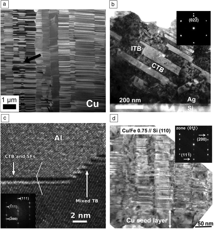
Although the sputtering technique has a much lower deposition rate than the PED technique, it can produce micron-thick NT metal films on Si substrates, which may see applications in the electronics industry.Reference Anderoglu, Misra, Wang, Ronning, Hundley and Zhang16Figure 1a shows a focused ion beam (FIB) microscopy micrograph of deformed NT Cu, where nanotwins are parallel to the substrate surface, also referred to as parallel growth twins, with an average twin spacing of 25 nm.Reference Hodge, Furnish, Shute, Liao, Huang, Hong, Zhu, Barbee and Weertman25 By using different substrates, inclined growth twins have been synthesized in sputtered epitaxial NT Ag (110) films on a Si (110) substrate with ∼40 nm average twin spacing (Figure 1b).Reference Bufford, Wang and Zhang20 By comparison, the average twin thickness in sputtered NT Ag (111) films is ∼10 nm at the same deposition rate and temperature.Reference Bufford, Wang and Zhang20

Figure 1. Microstructure of nanotwinned (NT) metals. (a) Focused ion beam microscopy micrograph showing a cross-sectional view of compressed NT Cu with an average twin spacing of 25 nm. Reprinted with permission from Reference Reference Hodge, Furnish, Shute, Liao, Huang, Hong, Zhu, Barbee and Weertman25. © 2012 Elsevier. Arrow indicates truncated twin column. (b) Cross-sectional transmission electron micrograph (TEM) of NT Ag (110) with inclined growth twins deposited on a Si (110) substrate. The average twin spacing is ∼40 nm.Reference Bufford, Wang and Zhang20 (c) Coherent twin boundary (CTB), stacking fault (SF), and incoherent twin boundary (ITB; mixed TB) in sputtered Al films.Reference Bufford, Liu, Zhu, Bi, Jia, Wang and Zhang26 (d) Sputtered fully coherent Cu/Fe 0.75 nm multilayers containing a high density of nanotwins. Fe has a face-centered-cubic structure in the multilayer.Reference Chen, Liu, Sun, Yu, Song, Wang and Zhang31 Insets show selected-area diffraction patterns.
The average twin spacing can also be tailored by controlling the orientation of growth twins by sputtering. Extending the applicability of NT microstructures to metals with high stacking-fault energy (SFE) or non-face-centered-cubic (fcc) structures remains a challenge, as it is energetically more difficult to introduce TBs in these materials. In this sense, the discovery of high-density growth twins in epitaxial Al comes as a surprise (Figure 1c).Reference Bufford, Liu, Zhu, Bi, Jia, Wang and Zhang26,Reference Bufford, Bi, Jia, Wang and Zhang27 The formation of growth twins in Al is assisted by a buffer layer with low SFE, and the epitaxial relation between the buffer and Al.Reference Bufford, Liu, Zhu, Bi, Jia, Wang and Zhang26 Similarly, high-density nanotwins have been introduced in other nanolayered materials,Reference Liu, Bufford, Wang, Sun and Zhang28–Reference Liu, Chen, Yu, Wang, Chen and Zhang30 including a NT Cu/Fe nanolayerReference Chen, Liu, Sun, Yu, Song, Wang and Zhang31 (Figure 1d), where Fe has a fcc structure and grows epitaxially with Cu.
Deformation in nanotwinned materials
Regardless of the growth technique used, TBs in NT fcc materials, including the {111} coherent twin boundary (CTB) and the {112} incoherent twin boundary (ITB),Reference Wang, Li, Anderoglu, Zhang, Misra, Huang and Hirth32 have been frequently observed (Figure 1). Understanding deformation mechanisms of NT metals has been a fertile research ground, where a principal focus has been understanding the role of TBs on mechanical properties of NT materials. The article by Sansoz et al. summarizes some of the major accomplishments in this area, and highlight work-hardening mechanisms enabled by CTBs in metallic nanowires.Reference Narayanan, Cheng, Zeng, Zhu and Zhu33
CTBs act as strong barriers to the transmission of dislocations due to slip discontinuity in association with the mirror symmetry, and strain hardening can be promoted by tailoring grain size, twin thickness, and temperature.Reference Zhang, Misra, Wang, Nastasi, Embury, Mitchell, Hoagland and Hirth19,Reference Lu, You and Lu34 Meanwhile, TBs are sinks for dislocations, as revealed by accumulation of high-density dislocations in NT metals (Figure 2a).Reference You, Li, Gui, Lu, Zhu, Gao and Lu35 N. Li et al. reported the pinning of mobile ITBs due to residual dislocations that were produced by transmission of glide dislocations across an ITB in Cu,Reference Li, Wang, Huang, Misra and Zhang36 and the formation of steps at CTBs due to dislocation-CTB interactions (Figure 2b).Reference Li, Wang, Misra, Zhang, Huang and Hirth37 Bufford et al. explored work hardening due to ITBs in NT Al (Figure 2c).Reference Bufford, Liu, Wang, Wang and Zhang38 Experiments showed that smaller twin spacing leads to greater strength, higher strain-rate sensitivity, enhanced work-hardening rate, and higher density of mobile dislocations at TBs in NT metals.Reference Zhang, Wang, Shan and Zhao9,Reference Cui, Han, Xin, Waryoba and Mbaruku14–Reference Wang, Sansoz, LaGrange, Ott, Marian, Barbee and Hamza21,Reference Hodge, Furnish, Shute, Liao, Huang, Hong, Zhu, Barbee and Weertman25,Reference Lu, Lu and Suresh39 In addition, softening in electrodeposited NT Cu occurs when twin spacing reduces to a few nm.Reference Lu, Chen, Huang and Lu40,Reference Li, Wei, Lu, Lu and Gao41
Figure 2. Strengthening and work hardening of nanotwinned (NT) metals. (a) Cross-sectional TEM of electrodeposited NT Cu subjected to a compressive strain of 5%. Twin boundaries (TBs) are decorated with dislocations.Reference You, Li, Gui, Lu, Zhu, Gao and Lu35 Inset shows a selected-area diffraction pattern of the material. (b) A high-resolution TEM snapshot from in situ nanoindentation of sputtered NT Cu. The interaction of a glide dislocation (indicated by “b”) with a coherent twin boundary (CTB) leads to steps at the CTB. Note: Numbers indicate atomic layers.Reference Li, Wang, Misra, Zhang, Huang and Hirth37 bF represents the Burgers vector of a Frank partial dislocation. (c) A TEM capturing the formation of steps due to dislocation pileups along an incoherent twin boundary (ITB) in NT Al during in situ nanoindentation.Reference Bufford, Liu, Wang, Wang and Zhang38 (d) Comparison of hardness for NT and polycrystalline Ag versus characteristic dimension. Data compiled from several studies.Reference Furnish and Hodge22,Reference Ott, Geng, Besser, Kramer, Wang, Park, LeSar and King23,Reference Bufford, Wang and Zhang42–Reference Fu, Shearwood, Xu, Yu and Khor48 Note: d, average grain size; t, average twin thickness; Leff, effective dimension considering both d and t (defined in text). The Hall–Petch slope for NT Ag calculated based on t alone is very different from the slope for polycrystalline Ag. When Leff is used, the Hall–Petch slope for NT Ag is similar to that of polycrystalline Ag.Reference Bufford, Wang and Zhang42
A compiled Hall–Petch (H–P) plot showing strength as a function of grain size for NT and polycrystalline Ag (Figure 2d)Reference Furnish and Hodge22,Reference Ott, Geng, Besser, Kramer, Wang, Park, LeSar and King23,Reference Bufford, Wang and Zhang42–Reference Fu, Shearwood, Xu, Yu and Khor48 suggests that the usage of average twin spacing alone may be insufficient to estimate size-dependent strengthening. For instance, the slope of the H–P plot for NT Ag (derived from the maroon dashed line in Figure 2d) based primarily on twin spacing (t) is much lower than the H–P slope for polycrystalline Ag with varying grain size (d) due to grain boundary (GB)-induced strengthening (blue dashed line in Figure 2d). In NT Ag, as both GBs and TBs contribute to strengthening, Bufford et al. derived the effective domain size (Leff) as a characteristic dimension in the H–P plot, where Leff is defined as:  $L_{eff} = d\left[ {1 - {t \over d} + {{\left( {{t \over d}} \right)}^2}} \right]$.Reference Bufford, Wang and Zhang42
Interestingly, such a parameter converts the scattered data (shown by half-open symbols in Figure 2d) for NT Ag to much more converged data points (represented by solid symbols). The H–P slope based on these converged data (shown by the red dashed line) is comparable to the H–P slope for polycrystalline Ag (blue dashed line). The general implication of this methodology needs further validation in other NT metallic materials.
Numerous molecular dynamics (MD) simulations have been performed to investigate deformation mechanisms of NT metals, and these have provided insights into TB-dictated plasticity at the atomic level. Mechanisms and mechanics of dislocation transmission across CTBs are dependent on the characteristics of the incoming dislocations and the applied stress. In slip transmission, an edge or mixed dislocation will transmit into the adjacent crystal across the CTB,Reference Wang and Huang49,Reference Jin, Gumbsch, Albe, Ma, Lu, Gleiter and Hahn50 while a screw dislocation often cross-slips on the CTB.Reference Zhu, Li, Samanta, Kim and Suresh51 Using in situ transmission electron microscopy (TEM) and MD simulations, N. Li et al. identified a novel dislocation multiplication mechanism when a mixed dislocation interacts with CTBs in Cu (Figure 2b), leading to steps with thicknesses of several atomic layers on the CTB.Reference Li, Wang, Misra, Zhang, Huang and Hirth37 The softening in electrodeposited NT Cu has been ascribed to abundant sources for dislocation nucleation when the twin spacing reduces to several nm.Reference Li, Wei, Lu, Lu and Gao41 For NT metallic nanowires, Sansoz et al. showed that strain softening occurs in metals with medium-to-high SFE, such as Al, whereas considerable work hardening occurs in metals with lower SFE (e.g., Ag and Au).Reference Deng and Sansoz52
Twinning effects on mechanical properties
The article by X. Li et al. focuses on fatigue, fracture, creep, and detwinning of NT metals. The majority of materials fail by fatigue or creep, hence it is important to investigate the mechanical response of NT metals under cyclic loading or constant stresses. Fatigue studies show that NT metals have enhanced fatigue resistance as compared with coarse-grained metals over a small number of cycles. However, the fatigue resistance of NT metals quickly decays over higher numbers of cycles.
Examination of fatigue-tested NT metals (Figure 3a) shows a decrease in the number of TBs, implying that detwinning occurs.Reference Yoo, Boles, Liu, Zhang, Schwaiger, Eberl and Kraft53 Detwinning has also been observed in NT metals subjected to high-pressure torsion (Figure 3b).Reference Shute, Myers, Liao, Li, Hodge, Barbee, Zhu and Weertman54 Furthermore, using in situ nanoindentation in a TEM, Wang et al. revealed that detwinning is accomplished by the migration of ITBs in NT Cu (Figure 3c).Reference Wang, Li, Anderoglu, Zhang, Misra, Huang and Hirth32 They further demonstrated that ITBs move via the migration of phase boundaries (considering an ITB is composed of a finite wide phase and two tilt GBs) in metals with low-to-intermediate SFE (Cu and Ni), while the migration of ITBs occurs via interface-disconnection glide mechanisms in Al with high SFE.Reference Wang, Misra and Hirth55 The stress required to migrate ITBs in Al is very high,Reference Bufford, Liu, Wang, Wang and Zhang38 as compared to that for ITB migration of fine twins in Cu.Reference Liu, Jian, Chen, Wang and Zhang56
Figure 3. Detwinning in nanotwinned (NT) metals under various deformation modes. (a) Detwinning in NT Cu subjected to a high-cycle fatigue test to 1.3 million cycles (a severely deformed region near crack edges).Reference Yoo, Boles, Liu, Zhang, Schwaiger, Eberl and Kraft53 (b) Partially detwinned NT Cu subjected to high-pressure torsion under a compressive stress of 3 GPa. Reprinted with permission from Reference Reference Shute, Myers, Liao, Li, Hodge, Barbee, Zhu and Weertman54. © 2011 Elsevier. (c) In situ nanoindentation study revealing the migration of incoherent twin boundaries (ITBs) in NT Cu. Transmission electron micrographs (c–e) illustrate the evolution of ITB migration; (f) shows the migration distance plotted versus time.Reference Wang, Li, Anderoglu, Zhang, Misra, Huang and Hirth32
Nanomechanical testing of nanotwinned materials
Various mechanical testing techniques have been applied to investigate the deformation mechanisms of NT metals. Among these, in situ nanomechanical testing has proven to be unique. N. Li et al. highlight several of these studies in their article. In particular, they summarize in situ nanoindentation studies in fcc Cu, Ni, and Al in order of increasing SFE.
In situ nanoindentation studies of Cu show that the interaction of dislocations with ITBs can lead to sessile dislocations that may pin the migration of ITBs.Reference Li, Wang, Huang, Misra and Zhang36 Alternatively, dislocations can interact with {111} CTBs, causing the multiplication of dislocations at TBs.Reference Li, Wang, Misra, Zhang, Huang and Hirth37 The stress for migration of ITBs in NT Cu is very low, ∼100 MPa, which is much lower than the yield strength of NT Cu.Reference Wang, Li, Anderoglu, Zhang, Misra, Huang and Hirth32,Reference Liu, Jian, Chen, Wang and Zhang56 The same technique also reveals substantial work hardening in NT Ni due to the formation of sessile dislocations at CTBs, where the CTBs effectively block the transmission of dislocations.Reference Lee, Holland, Mukherjee, Zhang and Wang57,Reference Zhu, Liao and Wu58 In situ nanoindentation studies of NT Al also show that ITBs provide strong barriers to the pileup of dislocations, which results in significant work hardening in NT metals in Al.Reference Bufford, Liu, Wang, Wang and Zhang38 They also highlight the finding of deformation twins in body-centered-cubic (bcc) metals such as W.Reference Wang, Zeng, Weinberger, Zhang, Zhu and Mao59
Deformation twinning in hexagonal materials
Deformation twinning is another important plastic deformation mode in crystalline materials. In general, high strain rates, low SFE, and low temperatures facilitate deformation twinning. Among the three common crystalline structures (bcc, fcc, and hcp), metals with hcp structure are most likely to form deformation twins when strained, because they rarely have a sufficient number of slip systems for an arbitrary shape change. Deformation twinning in hcp materials is directional, with a unique sense of shear, and results in the formation of a sheared domain, contributing to plastic deformation along the c-axis.Reference Christian and Mahajan2 The article by Liao et al. highlights several of these studies with a focus on the twinning system {10 $\overline1$2}〈10 $\overline{11}$〉, which is commonly activated in most hcp materials. The authors point out several technical challenges associated with deformation twinning in hcp materials.
Twin nucleation in hcp materials is driven by local stress states and local atomistic configurations at GBs. A twin nucleus must be comprised of multiple atomic layers for it to be stable,Reference Wang, Hirth and Tomé60 and nucleation occurs by a pure-shuffle mechanism, the so-called prismatic-basal (PB) transformation.Reference Wang, Yadav, Hirth, Tomé and Beyerlein61 This mechanism deviates from the classic dislocation-based nucleation mechanisms. Thus, a twin nucleus is surrounded by the PB interfaces instead of conventional CTBs. The discovery of PB interfaces has inspired research to revisit the topic of twin propagation and growth. High-resolution TEM analyses and atomistic simulations of TBs in hcp materials show that TBs are serrated and composed of both CTBs and PB/basal-prism (BP) boundaries.Reference Tu, Zhang, Wang, Sun, Liu and Tomé62,Reference Liu, Wang, Li, Lu, Zhang, Shan, Li, Jia, Sun and Ma63 Under some circumstances, the migration of BP/PBs can dominate twin growth, resulting in significant deviations of the TB away from the {10 $\overline1$2} plane.Reference Liu, Wang, Li, Lu, Zhang, Shan, Li, Jia, Sun and Ma63
Crystal plasticity-based approaches for modeling the constitutive behavior of hcp alloys have proliferated over the past decade. The crux of the problem has involved correctly accounting for the behavior of twinning and detwinning mechanisms in twin nucleation and propagation. MD simulations and microscopy characterizations indicate that nucleation of twins is preferred at low-angle GBs because of the available GB dislocations. Inspired by MD simulations, a breakthrough in mesoscale models was to introduce a twin nucleus through a stochastic process that is correlated to statistical distributions of GB dislocations and statistical perturbations of local stresses along GBs.Reference Beyerlein and Tomé64 Propagation/growth of twins is described through twin growth, twin shrinkage, and retwinning, while considering the stress relaxation associated with twin initiation and propagation.Reference Wang, Wu, Wang and Tomé65
Twin–twin interactions have also been investigated experimentally.Reference Yu, Wang, Jiang, McCabe, Li and Tomé66,Reference Yu, Wang and Jiang67 A twin is unlikely to transmit into another twin, thus correspondingly, twin–twin junctions are formed. Under cyclic loading, twinning and detwinning appear alternatingly. Figure 4a shows variation of twin volume fraction as a function of the number of loading cycles; the optical micrographs show twins at tensile and compression peak strains in the 40th, 400th, and 1610th loading cycles. After the 10th loading cycle, residual twins accumulate significantly. Large amounts of twin–twin interactions are formed in highly localized areas. These junctions impede continuous twinning due to the back stress and detwinning caused by the low-energy twin–TBs, leading to twinning-induced work hardening.Reference Yu, Wang, Jiang, McCabe, Li and Tomé66Figure 4b shows the stress-plastic strain hysteresis loops from the first to the 1610th loading cycle, revealing that the plastic strain contributed by twinning and detwinning gradually decreases with increasing loading cycles. At the same time, the critical stresses associated with twinning and detwinning gradually increase with increasing loading cycles (Figure 4c).
Figure 4. Cyclic hardening of a [0001]-oriented Mg single crystal subjected to fully reversed tension-compression at a strain amplitude of 0.5%. (a) Variation of twin volume fraction with respect to the loading cycles (red curve) together with optical micrographs showing twinning at tensile and compressive peak strains in the 40th, 400th, and 1610th loading cycles.Reference Yu, Wang and Jiang67 (b) Evolution of stress-plastic strain hysteresis loops from the first to the 1610th loading cycle. (c) Variation of the resolved shear stresses associated with twinning and detwinning, and their corresponding plastic moduli with the number of loading cycles.Reference Yu, Wang, Jiang, McCabe, Li and Tomé66
The pinning effect of solute atoms on TBs has recently attracted considerable attention. Periodic segregation of solute atoms at CTBs and PBs has been identified using scanning TEM.Reference Nie, Zhu, Liu and Fang68 Density function theory (DFT) calculations provide further insights for understanding solute solubility along CTB and PB/BP boundaries. Specifically, DFT calculations show that solute solubility has little dependence on the radius of solute atoms along CTB, but varies considerably with stresses on PBs.Reference Kumar, Wang and Tomé69
Twinning-induced plasticity steels
The twinning-induced plasticity (TWIP) effect enables the design of austenitic Fe-Mn-based steels that deform by a large amount of mechanical twinning accompanied by glide of dislocations. TWIP steels have outstanding mechanical properties at room temperature, as shown by a combination of high strength and ductility, and high work-hardening capacity.Reference Steinmetz, Jäpel, Wietbrock, Eisenlohr, Gutierrez-Urrutia, Saeed-Akbari, Hickel, Roters and Raabe70 The high strain-hardening coefficients are attributed to complex dislocation substructures and mechanical twinning that introduces TBs, refines the microstructure, and dynamically reduces the dislocation mean free path. The first TWIP steels (Fe-Mn-Si-Al steel) reported in 1998 had an ultimate tensile strength of 800 MPa with a total elongation of 85%.Reference Grässel and Frommeyer71 Recently, austenitic Fe-Mn-C-based TWIP steels have been synthesized with >70% elongation at an ultimate tensile strength >1 GPa.Reference Pierce, Jiménez, Bentley, Raabe, Oskay and Wittig72
TWIP steels typically have a high concentration of Mn (usually 20 wt% or greater) and small additions of elements such as C (<1 wt%), Si (<3 wt%), or Al (<3 wt%). The high concentration of Mn is crucial to preserve the austenitic structureReference Sato, Tanaka and Inoue73 and control the SFE of the Fe-based alloys.Reference Lee and Choi74 TWIP steels typically have low SFE (between 20 and 40 mJ/mReference Christian and Mahajan2) at room temperature. SFE in the steels can be tuned by adjusting alloy composition.Reference Pierce, Jiménez, Bentley, Raabe, Oskay and Wittig72 The close connection between alloy thermodynamics and substructure kinetics renders these steels an ideal model alloy family accessible to theory-based materials design. The article by Raabe et al. in this issue discusses and demonstrates the concept of theory-based design of TWIP steels.
Other properties of nanotwinned materials
A few other important topics relating to NT materials are not covered in this issue (Figure 5). TBs result in unique thermal stability of NT metals. With few exceptions, nanocrystalline metals generally have poor thermal stability, whereas, in contrast, NT metals have superior thermal stability.Reference Anderoglu, Misra, Wang and Zhang75–Reference Zhao, Furnish, Kassner and Hodge77 The TB energy is normally an order of magnitude lower than that of a high-angle GB, and hence the driving force for coarsening of twins is significantly lower than that for grain coarsening in nanocrystalline metals. Consequently, after annealing at high temperatures, NT metals remain strong, while nanocrystalline metals soften significantly (Figure 5a).Reference Anderoglu, Misra, Wang and Zhang75–Reference Zhang, Misra, Wang, Swadener, Lima, Hundley and Hoagland81
Figure 5. Other characteristics of nanotwinned (NT) metals. (a) NT metals are more stable than nanocrystalline and ultrafine-grained metals at higher temperature (as indicated by retention of high hardness after annealing) because coherent twin boundaries (CTBs) store much lower energy than high-angle grain boundaries.Reference Anderoglu, Misra, Wang and Zhang75–Reference Zhang, Misra, Wang, Swadener, Lima, Hundley and Hoagland81 T/Tm is the normalized annealing temperature. Tm is the melting temperature of metals. (b) NT Cu has higher hardness and higher electrical conductivity than nanocrystalline Cu.Reference Lu, Shen, Chen, Qian and Lu8,Reference Cui, Han, Xin, Waryoba and Mbaruku14,Reference Anderoglu, Misra, Wang, Ronning, Hundley and Zhang16,Reference Anderoglu, Misra, Ronning, Wang and Zhang83–Reference Smithells and Brandes90 (c) In situ Kr ion irradiation studies (inside a transmission electron microscope) show that CTBs in NT Ag destruct stacking-fault tetrahedra (SFT).Reference Yu, Bufford, Sun, Liu, Wang, Kirk, Li and Zhang91 Yellow lines outline the truncated SFTs. (d) The density of SFTs decreases with decreasing average twin spacing for a NT Ag specimen irradiated with the same dose.
A model was developed to understand the formation of nanoscale growth twins in sputtered Cu.Reference Zhang, Misra, Wang, Shen, Nastasi, Mitchell, Hirth, Hoagland and Embury82 A recent study of NT Ag shows that texture can also tailor the formation of twins.Reference Bufford, Wang and Zhang20 Besides good thermal stability, certain NT metals (such as Cu) also have high electrical conductivity and high strength (Figure 5b).Reference Lu, Shen, Chen, Qian and Lu8,Reference Cui, Han, Xin, Waryoba and Mbaruku14,Reference Anderoglu, Misra, Wang, Ronning, Hundley and Zhang16,Reference Anderoglu, Misra, Ronning, Wang and Zhang83–Reference Smithells and Brandes90
The electron scattering coefficient at CTBs is an order of magnitude lower than that at GBs; CTBs provide a unique way of enhancing strength with little loss of electrical conductivity.
Recently, it has been shown that NT metals such as Cu and Ag also show excellent radiation resistance (Figure 5c–d).Reference Yu, Bufford, Sun, Liu, Wang, Kirk, Li and Zhang91–Reference Yu, Bufford, Khatkhatay, Wang, Kirk and Zhang94 Although stacking-fault tetrahedra (SFTs) are frequently generated in NT metals, CTBs and ITBs can effectively engage and eliminate SFTs. Therefore, they significantly reduce the density of defect clusters in heavy ion-irradiated NT metals.Reference Yu, Bufford, Sun, Liu, Wang, Kirk, Li and Zhang91,Reference Li, Yu, Chen, Song, Wang, Kirk, Li and Zhang92
Conclusion
The aim of the articles in this issue of MRS Bulletin is to summarize and highlight prior studies as well as our current understanding of twinning, and to outline the significant scientific and technological challenges in front of us. Although this issue pertains primarily to twinning in metallic materials, these articles may have implications for scientific studies on twinning in other types of materials, such as twinned alloys and ceramic materials.
Although the mechanical behavior of twinned metals has been intensely investigated, scientific challenges remain. The influence of defective TBs on deformation mechanisms and plasticity of NT metals are not well understood. Most prior studies on NT metals focus on monolithic metal systems, thus there are abundant opportunities to investigate the synthesis and mechanical properties of NT alloys. As detwinning frequently occurs in monolithic metals and leads to softening and reduced fatigue resistance, it is important to enhance mechanical stability of TBs. In situ nanoindentation studies on mechanical behavior of NT metals at atomic resolution remain scarce. An in-depth understanding of the mechanisms and mechanics of deformation twinning in hcp materials and TWIP steels, such as nucleation, propagation/growth, dislocation–twin, and twin–twin interactions, is also essential.
The methodologies that integrate the alloy design (first-principle calculation) approach into multiscale plasticity modeling may provide effective routes to discover novel twinned metallic materials and to understand the influence of twinning and nanotwins on their mechanical properties.
Acknowledgments
J.W. would like to thank the US Department of Energy, Office of Science, Basic Energy Sciences, Materials Sciences and Engineering Division for their support. X.Z. acknowledges financial support by DoE-OBES under Grant No. DE-SC0010482. He also acknowledges contributions by his former graduate students, Osman Anderoglu, Nan Li, Yue Liu, Youxing Chen, Daniel Bufford, and Kaiyuan Yu, and long-term collaborators, Amit Misra, John Hirth, and Haiyan Wang. Access to the DOE-Center for Integrated Nanotechnologies at Los Alamos and Sandia National Laboratories and the microscopes at the Microscopy and Imaging Center at Texas A&M University are also acknowledged.